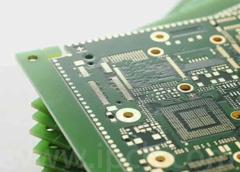
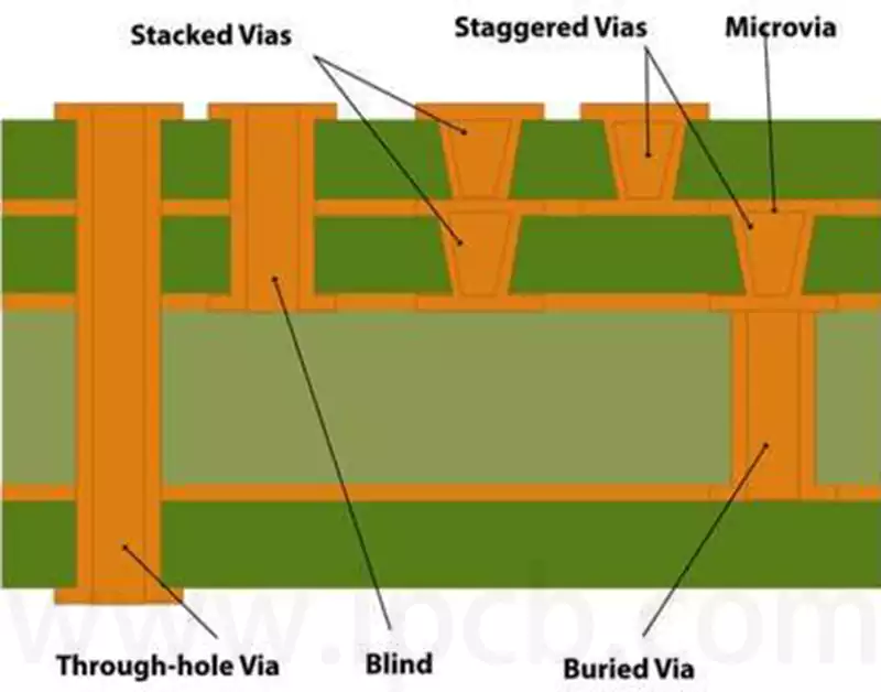
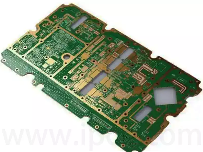
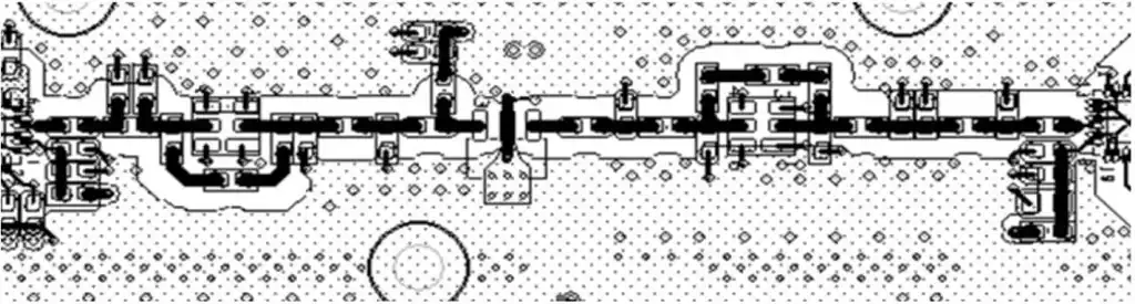
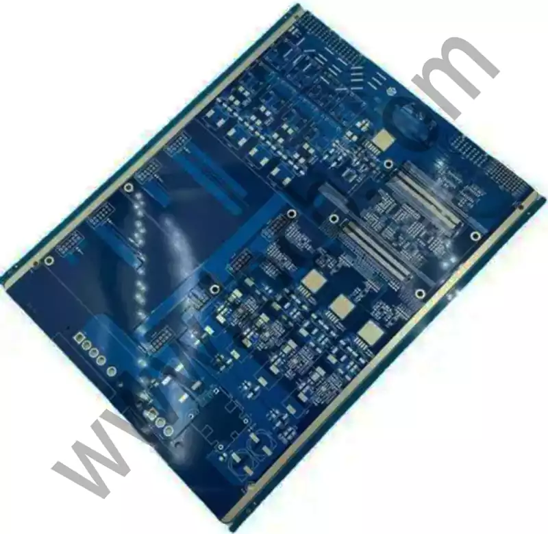
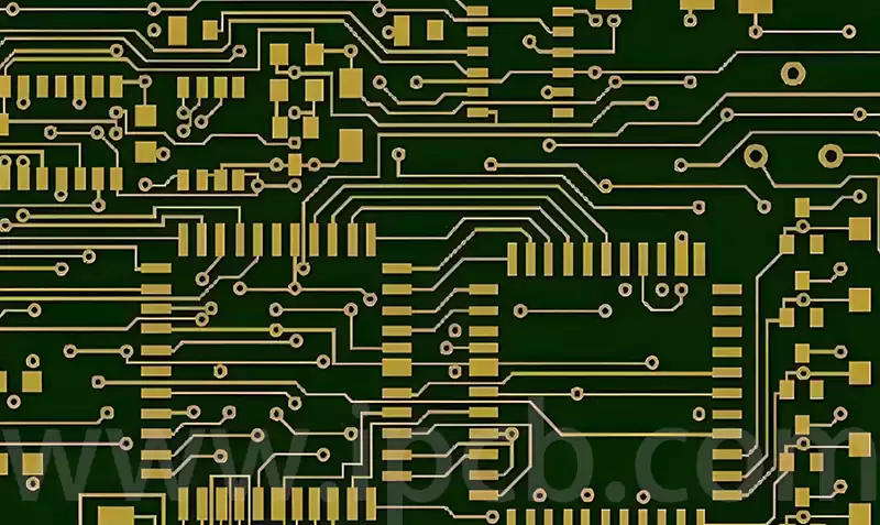
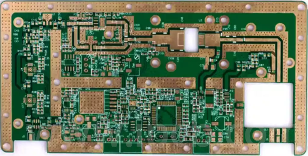
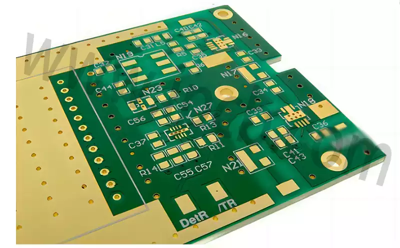
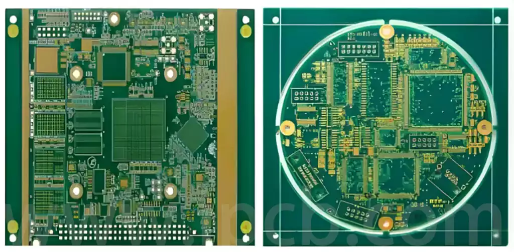
Electronic manufacturer

printed circuit board heat exchanger

Printed Circuit Board Heat Exchanger

The Printed Circuit Board Heat Exchanger (PCB-HEX) is a highly efficient compact heat exchanger manufactured using printed circuit board technology, which is characterised by the fact that the metal wires and tubes are printed directly onto a thin-film substrate, and the structural design is similar to that of a traditional printed circuit board, hence the […]

how much does a pcb board cost

How much does a pcb board cost

While it is true that there are some generally applicable basic processes in the PCB board industry, it is even more critical to carefully select and determine the appropriate production processes and equipment based on the thickness and material of the substrate, the precise standard of line width and spacing, the design architecture,the scale of

pcba

PCBA processing requirements for PCB boards

In the field of electronics manufacturing, PCBA chip processing constitutes a core link in the product manufacturing process, and plays a decisive role in the performance, stability and durability of electronic products. Stability and durability play a decisive role in the performance of electronic products, stability and durability.PCBA chip processing of pcb boards set a

pcb soldering

Double Sided PCB Soldering Tips

PCB soldering precautions1.EDA365 electronic community suggests that the first task after obtaining the PCB bare board is to carry out visual inspection to confirm that there are no short circuits, broken circuits and other defects, and in-depth understanding of the development board schematic, and PCB screen printing layer carefully compared to ensure that the two

double sided pcb board

Double sided pcb board manufacturing process challenges

The production process for double sided pcb board​ consists of several stages, each of which may face a number of technical challenges.The following are some of the major challenges: Design complexity:Double sided pcb board​ require circuitry to be laid out on two levels,which greatly increases the difficulty of the design.Designers must ensure that the circuits

PCBA

PCBA SMD preparation and processing considerations

PCBA chip processing is one of the core links in the manufacturing process of electronic products, which includes a number of stages from circuit design to product moulding. Each stage needs to be carefully prepared to ensure that the production process is carried out smoothly, as well as the quality and reliability of the final

What does ctr stand for on a pcb​

What does ctr stand for on a pcb​

What does ctr stand for on a pcb? The current transfer ratio (CTR) is a critical parameter in electronic design and component selection, especially in optocouplers, where CTR not only determines the performance of the optocoupler, but also affects the stability and efficiency of the overall circuit. The current transfer ratio (CTR) refers to the

can you use ac in a pcb

Can you use ac in a pcb

Can you use ac in a pcb? Circuit boards can use either AC or DC as a power source, depending on the design and purpose of the board. Some circuit boards require AC power, such as televisions and stereos in household appliances, which require AC power to function properly. And some circuit boards require the

PCB Pad

PCB pad types and their design guidelines

In PCB design,pads as a bridge connecting components and circuit boards, its type and design standards are critical. Different types of pcb pads are suitable for different components and application scenarios, while reasonable design standards ensure soldering reliability and board performance. Common pcb pad types:Square pads: suitable for large and small number of components, as

pcb radar

Introduction of PCB radar

PCB radar is a circuit board specially designed for use in radar systems to connect and support various electronic components and devices in the radar system. It plays a key role in the radar system to enable proper operation and efficient performance of the radar system. Common materials for pcb radarThe choice of material for

copper oxydation pcb no solder mask

Copper oxydation pcb no solder mask

Copper oxydation pcb no solder mask is a special type of printed circuit board that protects the copper conductors by forming a stable copper oxide film instead of a solder mask. This oxide layer not only enhances the corrosion resistance of the pads, but also improves solder wetting, ensuring that the solder material adheres better

tin plating

Tin plating technology for circuit board

What is tin plating?Tin plating is the application of a layer of tin to a copper foil. In the circuit board manufacturing process, the surface of the copper foil is immersed in a solution containing tin salts,and a uniform layer of tin grows on the surface of the copper foil through an electrolytic reaction. Tin

pcb copper foil

Thickness of pcb copper foil

In PCB (Printed Circuit Board) manufacturing, an ounce (OZ) is essentially a unit of weight, which converts to grams (g) roughly as follows: 1 OZ equals approximately 28.35 g. The term 1 OZ refers specifically to the thickness of 1 OZ of copper uniformly covered over an area of 1 square foot (FT2). The term

remove solder from

Remove solder from pcb to quality assurance

Solder flux residue is generally defined as the residual material left on the surface of a circuit board or other workpiece during a soldering operation or electronics manufacturing process due to the use of soldering materials (e.g., solder or solders), through-hole soldering, and by-products generated during the soldering process. These residual components may include solder

standard PCB thickness

What is industry standard PCB thickness?

What is industry standard PCB thickness?The standard PCB thickness for 2 layers is 1.6mm.Depending on the specific requirements of the design, measurements other than the standard measurements are used in the PCB design. Typically PCB thicknesses range from 0.2mm to 3.2mm. 0.2mm PCB standard thickness is used for thin and flexible PCBs, but on the

light emitting diode

How to check light emitting diode with multimeter

An LED (light emitting diode) is a semiconductor diode,specifically a p-n junction, that emits light when a positive current flows from the anode (labelled ‘+’, i.e., positive) to the cathode (labelled ‘-’, i.e., negative). The symbol of the diode is usually represented by an arrow that meets the vertical line at the front end,and the

common components on a PCBA

Overview of common components on a PCBA

PCBA processing is the core process of circuit board manufacturing, covering the two main aspects of PCB manufacturing and SMT placement processing, in which the addition of electronic devices is indispensable. Electronic devices are not only the basic elements of PCBA processing, but also play a decisive role in the performance and quality of the

normal keyboard pcb

Functions of a normal keyboard PCB

A normal keyboard PCB, also known as a printed circuit board (PCB), is an essential component of the keyboard’s internal structure. It plays the role of receiving the user’s instructions and converting them into electronic signals that are recognized by the computer. When the user touches any key on the keyboard, the corresponding switch is

flying probe

Flying probe test for PCB measurement

Flying probe testing is a method of testing electronic circuits, primarily for testing printed circuit boards (PCBs). It utilizes a system of movable probes that actually “fly” across the board, making electrical contact with specific test points on the PCB. Ultimately, it identifies defects and verifies the electrical performance of the circuit. A flying probe

solder mask

PCB solder mask selection and application

Solder mask is a key technology in the manufacture of PCBs (Printed Circuit Boards), designed to protect the metal components of the board from oxidation and to avoid the formation of conductive bridges between the pads. Soldermask is particularly important in processes such as reflow or wave soldering, where it is difficult to precisely control

glass pcb

Glass pcb and TGV carrier board manufacturing process

Glass pcb and their derivatives, glass through hole (TGV) carrier board,has become indispensable core components for various high-tech electronic products. They are not only widely used in liquid crystal display (LCD),organic light-emitting diodes (OLED) and other display technologies,but also play an important role in semiconductor packaging, integrated circuit interconnections and other aspects. Mainstream manufacturing techniques

countersunk hole

Countersunk hole in PCB applications and manufacturing

A countersunk hole is a semi-penetrating hole in a circuit board made with a flat head drill or gong cutter, characterised by the fact that the hole does not run through the entire circuit board. Between the outer edge of the hole (i.e., the location of the largest hole diameter) and the wall of the

pcba(printed circuit board)

PCBA IC Pin Moulding Process

PCBA (Printed Circuit Board Assembly) integrated circuit lead forming process is an important technology in modern electronics manufacturing, which involves adapting the pins of integrated circuits to the specific shape and requirements of the board. This process plays a key role in ensuring pin soldering and product performance, which not only affects production efficiency, but

ic design

Semiconductor IC Design

Semiconductor IC design (Integrated Circuit Design) refers to the design process of integrating multiple devices and functional modules on a wafer and connecting and interconnecting them efficiently based on semiconductor processes and in accordance with certain circuit design rules and principles. Typically, semiconductor IC design involves a number of sub-fields,including digital circuit logic design.Analogue circuit

Scroll to Top