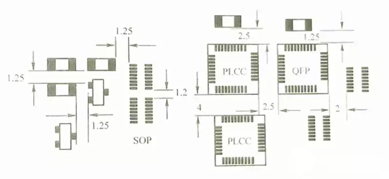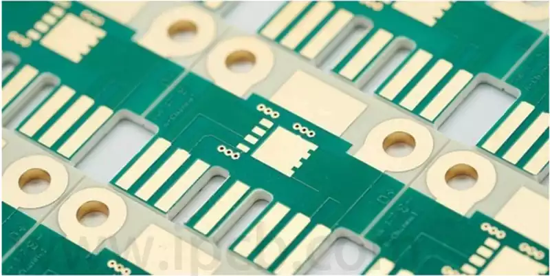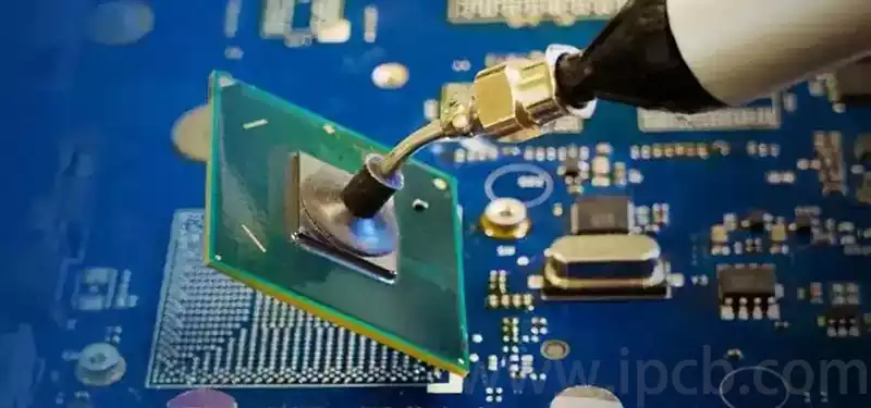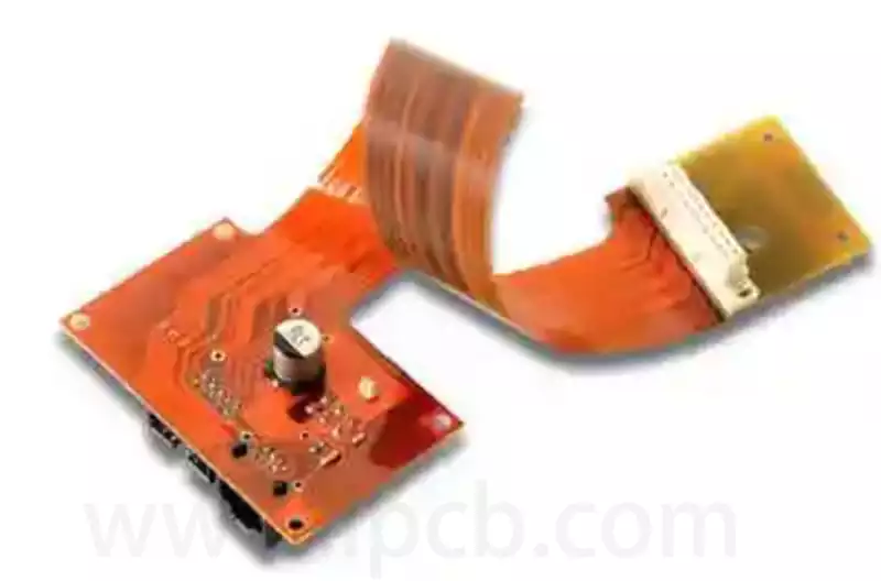
FPC PCB Assembly Process
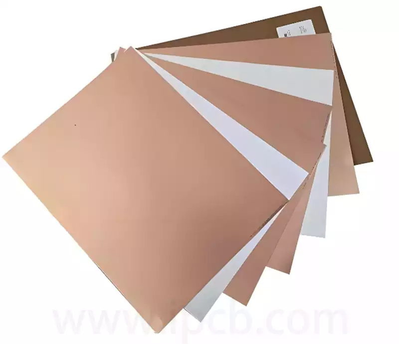
There is a significant difference between FPC PCB assembly and the assembly of rigid circuit boards, the main reason is that flex board is softer and less hard, if you do not use a special carrier board, it is difficult to achieve effective fixation and handling, so as to be unable to complete the printing, […]