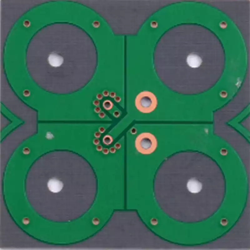
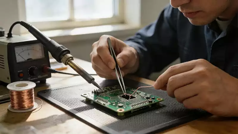
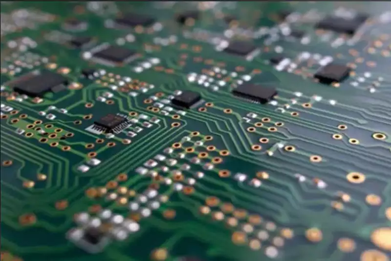
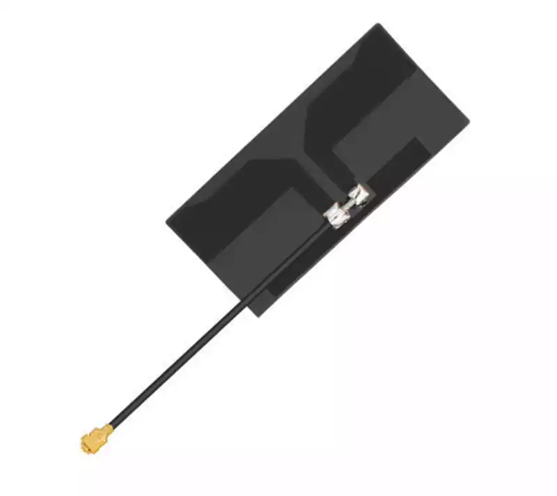
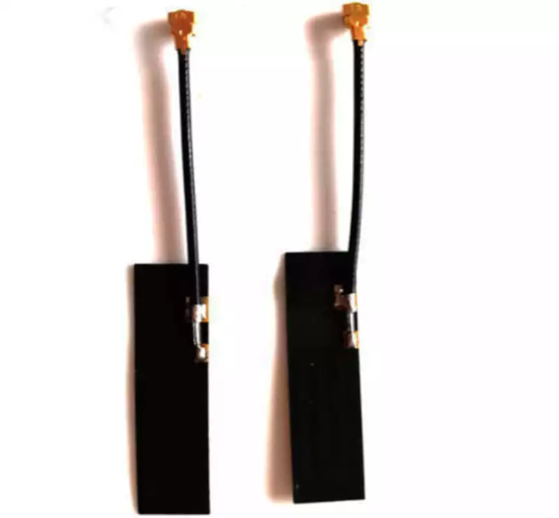
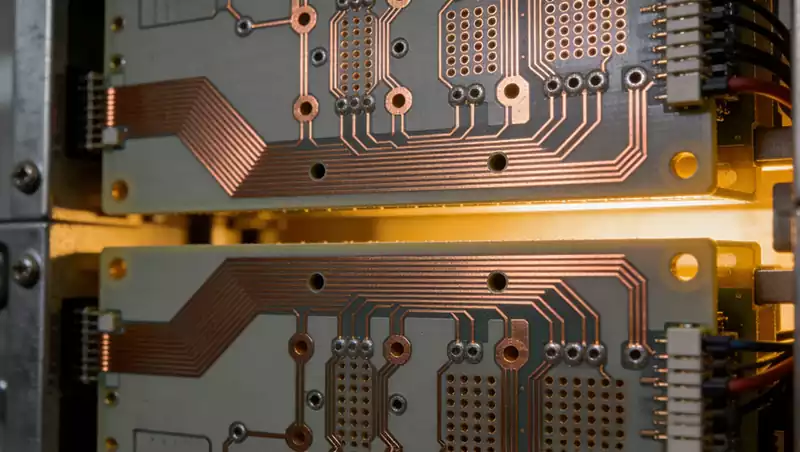
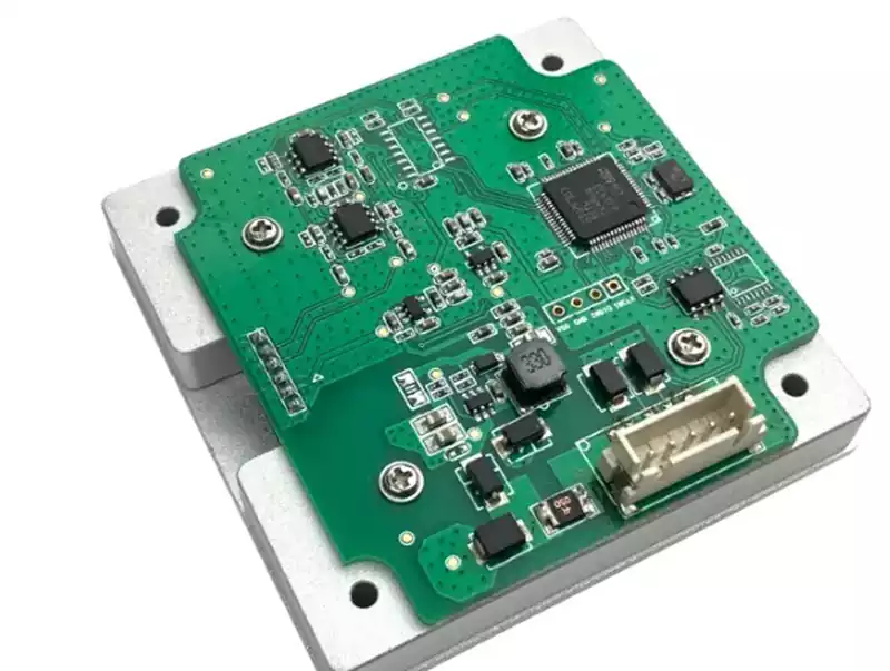
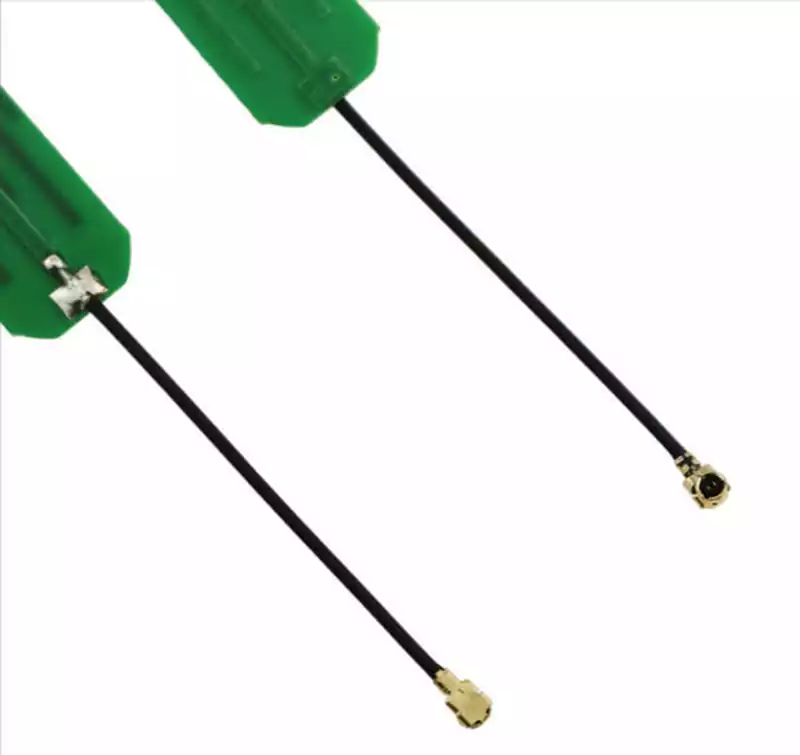
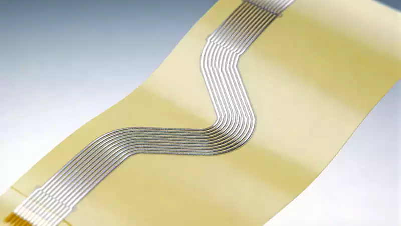
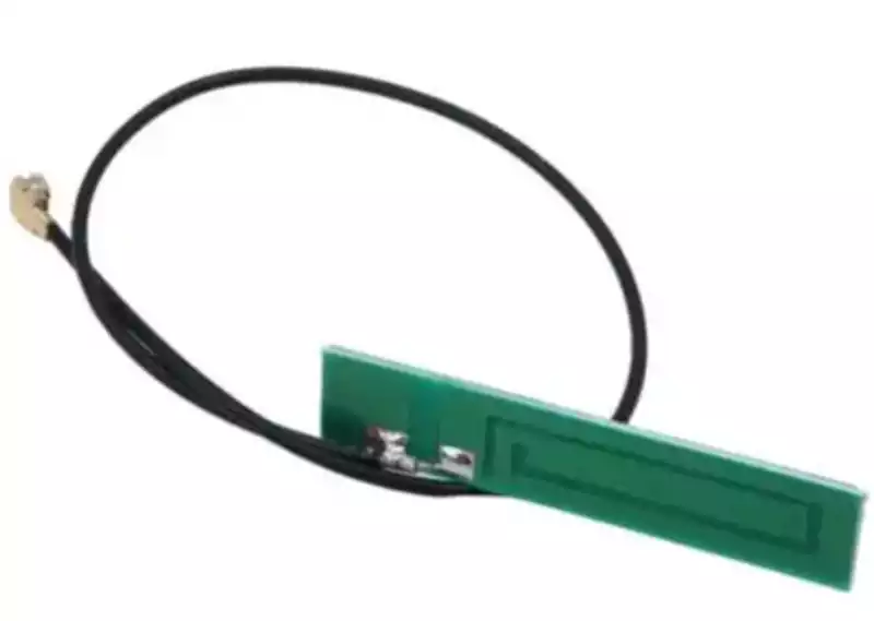
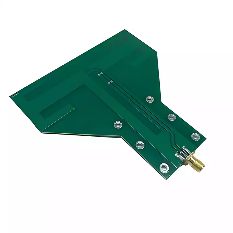
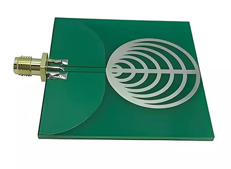
Electronic manufacturer

pcba

Key Factors Affecting PCBA Processing Costs and Quotation Efficiency

PCBA processing costs encompass multiple stages including PCB manufacturing, component procurement, SMT placement, DIP insertion, and testing/validation. Quotation efficiency is influenced by factors such as design file completeness, supply chain alignment, process complexity, batch size, and testing requirements. This article systematically outlines the cost components of PCBA and analyses key factors affecting quotation timeliness. PCBA […]

cold solder joints

Detection and Prevention of Cold Solder Joints in PCB Board

Cold solder joints refer to instances during the soldering process where an inadequate metallic bond forms between the solder and the workpiece. While appearing connected, such joints exhibit poor contact, severely compromising the performance and reliability of electronic products and potentially causing product failure. Accurate detection and effective remediation of cold solder joints are crucial

Microwave Radio Frequency

Principles and Applications of Microwave Radio Frequency Technology

Microwave radio frequency technology refers to techniques utilising radio waves within the frequency range of 300MHz to 300GHz for information transmission, processing, or application. Radio frequency (RF) typically denotes electromagnetic waves across a broad spectrum, while microwaves constitute the higher-frequency, shorter-wavelength segment within this range. Owing to characteristics such as high frequency, rapid transmission, substantial

Microwave RF PCB​

Characteristics and Applications of Microwave RF PCB​

Microwave RF PCB refers to microwave components manufactured using conventional rigid PCB fabrication methods on specific microwave-grade copper-clad laminates. In printed circuit board wiring for high-speed signal transmission lines, products can currently be categorised into two main types: one category comprises electronic products for high-frequency signal transmission. These products relate to radio electromagnetic waves and

millimeter-wave radar

PCB Design and Material Selection for 4D Millimeter-Wave Radar

4D millimeter-wave radar represents an upgrade from conventional millimetre-wave radar, with “4D” denoting four dimensions: velocity, distance, horizontal angle, and vertical height. Compared to conventional 3D millimeter-wave radar, 4D millimetre-wave radar incorporates the detection of ‘height’, integrating this fourth dimension into traditional systems. This enables 4D millimeter-wave radar to: 1) Acquire information across richer dimensions,

PCB materials

Key Performance Characteristics of PCB Materials for 77GHz Automotive Radar

The significance of high-frequency PCB materials in 77 GHz automotive radar applications. Within the high-frequency spectrum, although numerous novel PCB materials have been developed, not all are suitable for such elevated frequencies. At millimetre-wave frequencies, which PCB material characteristics prove most critical? Understanding these properties facilitates the simplification of millimetre-wave applications, particularly concerning the selection

flexible printed circuit board

Differences in Layout and Routing for Single- and Double-Sided Flexible Printed Circuit Boards

Flexible printed circuit boards (FPCs), serving as core components for interconnecting electronic devices, have their layer count design directly impacting product performance, cost, and application scenarios. Based on the number of conductive layers, FPCs can be categorised into single-layer, double-layer, and multi-layer (three layers and above) structures. Flexible pcb with different layer counts exhibit significant

flexible LED strip lights

Features and Advantages of Flexible LED Strip Lights

Flexible LED strip lights, also known as flexible ribbon lights, utilise FPC as the substrate circuit board and are assembled with surface-mount LEDs, resulting in a product thickness of merely 0.1cm that occupies minimal space. Common specifications include 30 LEDs per metre, 60 LEDs per metre, 120 LEDs per metre, 144 LEDs per metre, and

High frequency PCB

High Frequency PCB Design and Manufacturing Challenges and Solutions

With the rapid proliferation of electronic products and the swift advancement of technology, demand for high-frequency, high-speed printed circuit boards continues to grow. High frequency PCB plays a pivotal role in modern communications, radar systems, and high-speed data processing. However, their unique high-frequency characteristics and stringent requirements for signal integrity render the manufacturing of high-frequency

multilayer flex pcb

Manufacturing Techniques And Challenges For Multilayer Flex PCB

Multilayer flex pcb is formed by laminating three or more layers of single-sided or double-sided flexible circuit boards together. Through-holes are created via drilling and plating, establishing conductive pathways between different layers. This eliminates the need for complex soldering processes. Whilst the number of conductive layers in such flexible designs can be virtually unlimited, layout

flexible pcb assembly

Applications and Technical Challenges of Flexible PCB Assembly

Flexible PCB assembly refers to circuit boards manufactured using flexible substrates, offering superior bendability and adaptability compared to traditional rigid PCBs. Flexible PCB assembly enables higher-density routing, saving space and making it suitable for devices with complex geometries. Flexible PCB assembly possesses the following characteristics and advantages:Flexibility and BendabilityFlexible PCB assembly can be freely bent,

Photoresist

The Application of Photoresist in Electronics Manufacturing

Photoresist, also known as photo-resistive material, refers to an etch-resistant thin-film material whose solubility changes upon exposure to ultraviolet light, electron beams, ion beams, X-rays, or other forms of radiation. Photoresist comprises photosensitive resin, photoinitiators, solvents and additives: photoinitiators, also known as photopolymerisation materials (primarily including UV coatings, UV inks, UV adhesives, etc.), are materials

pcb jumper

Key Considerations for Fabricating PCB Jumper

PCB jumper refers to spaces reserved on a printed circuit board for connecting circuits, achieved by adding conductive wires and connectors. They serve a broad purpose in circuit design, effectively resolving layout and routing challenges. Jumpers serve as ‘circuit shortcuts’ in PCB design, achieved through thickened conductors or special connection methods, specifically addressing the following

pcb circuit board

Distinction between Lead-Free and Leaded Hot Air Reflow Processes for PCB Circuit Boards

The surface treatment process of PCB circuit boards is crucial to their performance and environmental credentials. Among these, the tin-plating process is widely favoured for its cost-effectiveness and solderability. Tin-plating can be categorised into leaded and lead-free variants based on lead content, exhibiting significant differences in composition, soldering characteristics, environmental requirements, and application scenarios. What

leadfree processes

What are leaded and leadfree processes?

What are leaded and leadfree processes? Leaded solder typically consists primarily of tin-lead (Sn-Pb) alloys, such as the classic Sn63/Pb37 (63% tin, 37% lead), which has a low melting point (approximately 183°C), stable soldering properties, and a mature process. Lead-free solder, conversely, primarily utilises alloys such as tin-silver-copper (e.g., SAC305) or tin-copper (Sn-Cu), which are

encapsulation process

Semiconductor encapsulation process and development

The encapsulation process, also known as the packaging process, involves the secure enclosure of semiconductor chips using specific materials. This provides effective defence against environmental degradation, ensuring stable chip operation. Beyond delivering crucial physical protection, the process is designed from the outset to fully account for the inherent characteristics of chips – namely their lightweight,

pcb board

Differences Between Multilayer and Double-Layer PCB Board

As electronic products demand increasingly diverse functionalities, pcb board structures have grown ever more complex. Constrained by spatial limitations, PCB circuit boards have progressively “evolved” from single-layer to double-layer and ultimately multi-layer designs. What, then, distinguishes the manufacturing processes of multi-layer PCB boards from those of double-layer PCBs? A multilayer pcb board is a type

ionic cleanliness

Ionic cleanliness Testing Methods and Importance for PCB Boards

Ionic cleanliness testing serves as a critical quality control measure for evaluating ionic contaminant levels on pcb boards surfaces. Its primary objective is to prevent electrical faults such as short circuits and corrosion caused by ionic residues, thereby enhancing the reliability of electronic products. Employing techniques such as chemical extraction and conductivity measurement, this test

fr1 pcb

Characteristics and Applications of FR1 PCB

FR1 pcb is constructed from glass fiber-reinforced epoxy resin laminates. FR1 PCBs are rigid, flat materials composed of thin copper layers on a non-conductive phenolic resin substrate. FR1, fully known as Flame Retardant 1, is a PC film with high insulation and flame-retardant properties. This material not only exhibits excellent flame resistance but also possesses

PCB laser depaneling

Application and Advantages of PCB Laser Depaneling Technology

In electronic manufacturing, circuit boards must be divided into distinct sections to meet the design requirements of various electronic products. Traditional mechanical cutting and punching techniques struggle to satisfy modern production standards. The advent of PCB laser depaneling machines has made this process efficient and precise, not only boosting production efficiency but also ensuring the

osp

OSP process ensures stable PCB performance

OSP (Organic Solderability Preservative) is a surface treatment process for PCBs (Printed Circuit Boards). It involves coating the copper foil surface with an extremely thin organic protective film (approximately 0.2-0.5μm thick) to prevent copper oxidation and maintain solderability. During soldering, high temperatures cause the protective film to decompose, exposing the copper surface to bond with

pcba

Methods and Significance of PCB Board Ion Cleanliness Testing

Ion cleanliness typically refers to the ion cleanliness of pcb board. Residual ions from various materials during the cleaning process can compromise the functionality and reliability of electronic products. Common issues arising from ionic contamination include surface corrosion and crystalline growth, ultimately leading to short circuits. Excessive current flow through connectors may result in the

fpc

The Role and Challenges of FPC in the 5G Era

What does FPC stand for? FPC stands for Flexible Printed Circuit, known in Chinese as a flexible printed circuit board, commonly abbreviated as a flexible board. FPC is a highly reliable, exceptionally flexible printed circuit board manufactured using polyimide or polyester film as the substrate material, also referred to as a flexible circuit board or

pcba

PCBA Component Spacing Design

Component spacing design on PCBA represents a pivotal aspect of electronic product development, where precision directly influences circuit electrical performance, thermal efficiency, manufacturing feasibility, and the stable operation of the final product. Component spacing is not merely a matter of spatial allocation, but rather an art form that comprehensively considers electrical safety, thermodynamics, signal integrity,

Scroll to Top