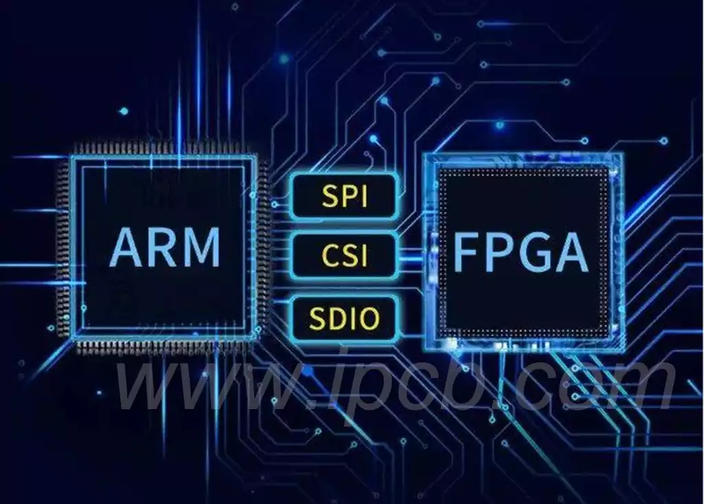
The HDI Process Advancement and Application
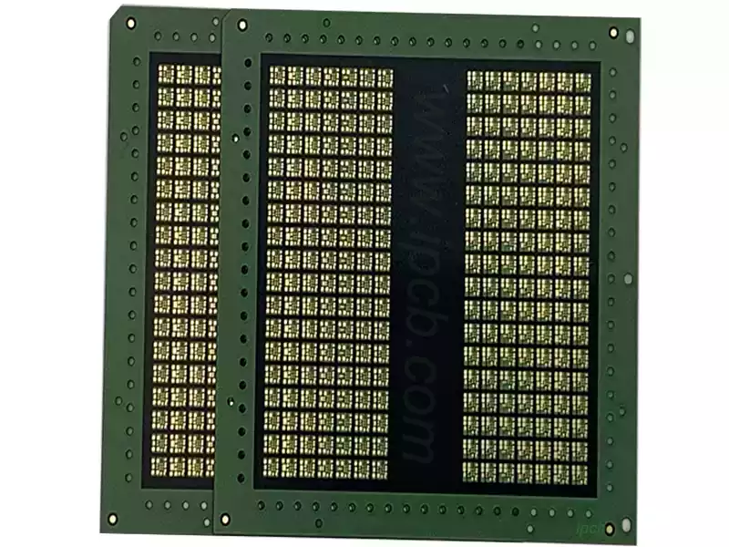
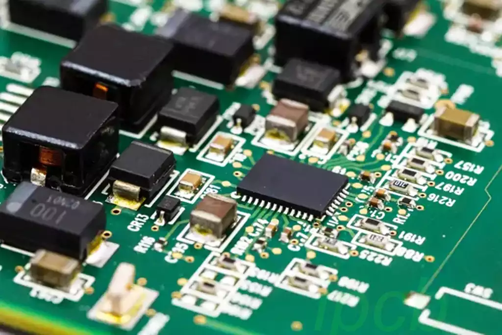
HDI step refers to the complexity of the manufacturing process of HDI boards, generally with the accumulation of layers (Build-up) to manufacture HDI boards, the more the number of layers, the higher the HDI process, the higher the technical grade of the board is also higher. HDI order can be divided into the following categories.HDI […]