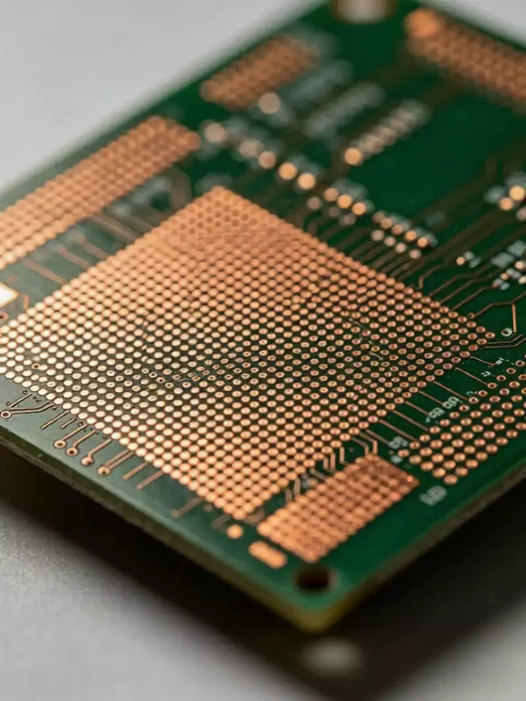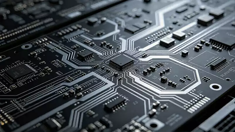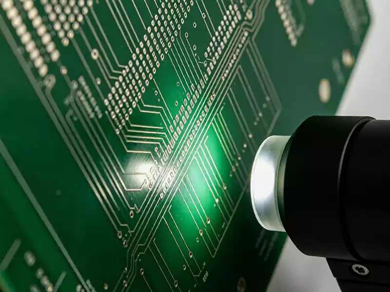
Key Points of FCT Testing
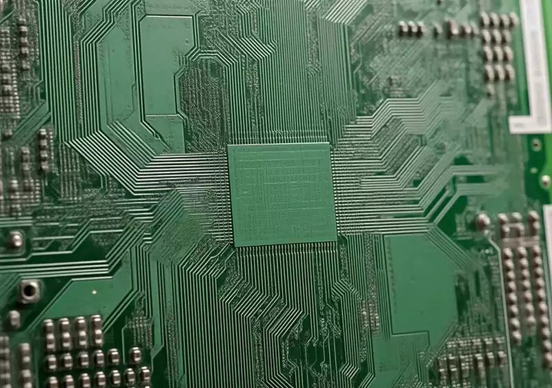
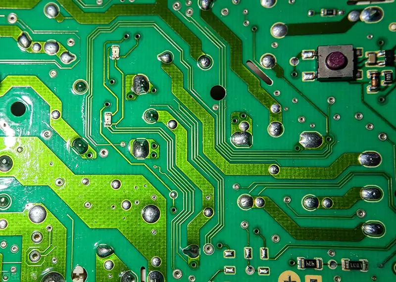
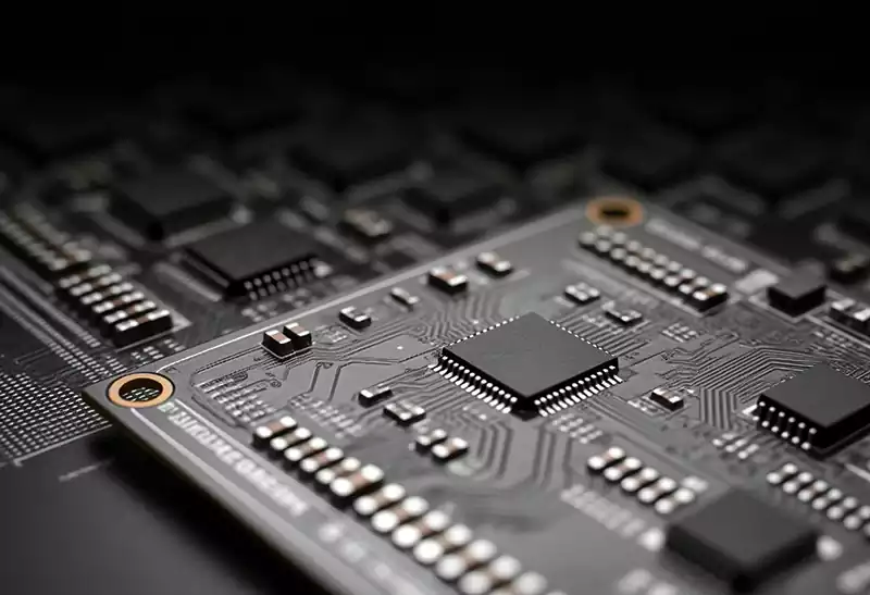
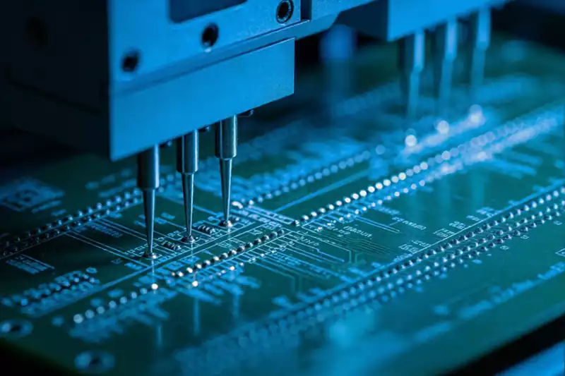
What is FCT testing? The core principle of FCT (Functional Circuit Test) is to treat the PCBA as a complete functional module, simulate its actual operating environment within the end product, apply real-world input signals, and verify whether the output response meets design requirements. Put simply, it involves providing the Unit Under Test (UUT) with […]