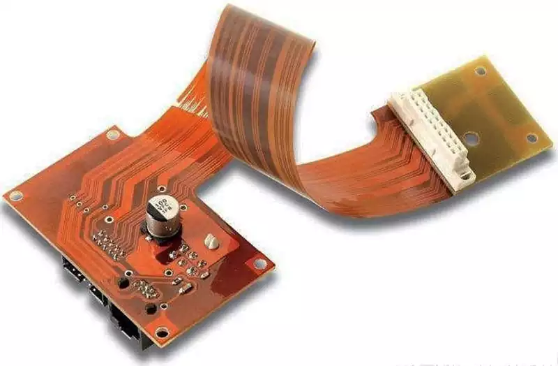
Factors affecting FPC pricing
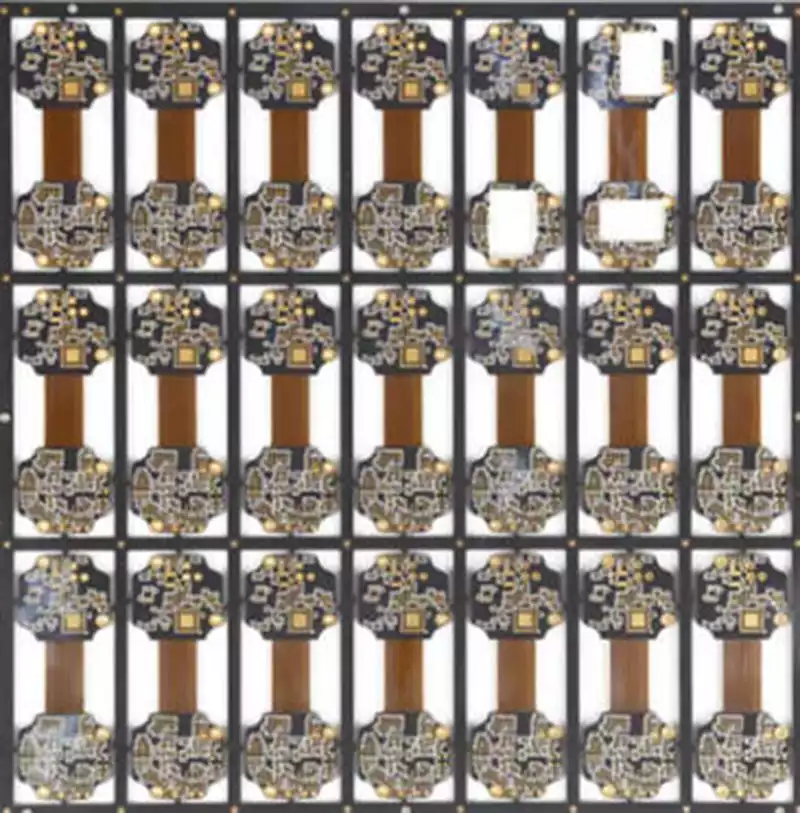
FPC quotations are influenced by a combination of four key factors: materials, structural design, manufacturing requirements and order volume. Any variation in the selection or specifications of these elements will be directly reflected in the final price. MaterialsMaterial costs form the core component of FPC quotations, accounting for 30% to 50% of the total. Differences […]