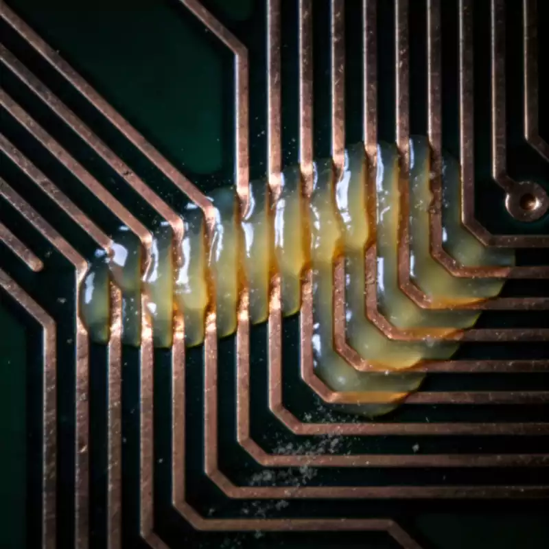
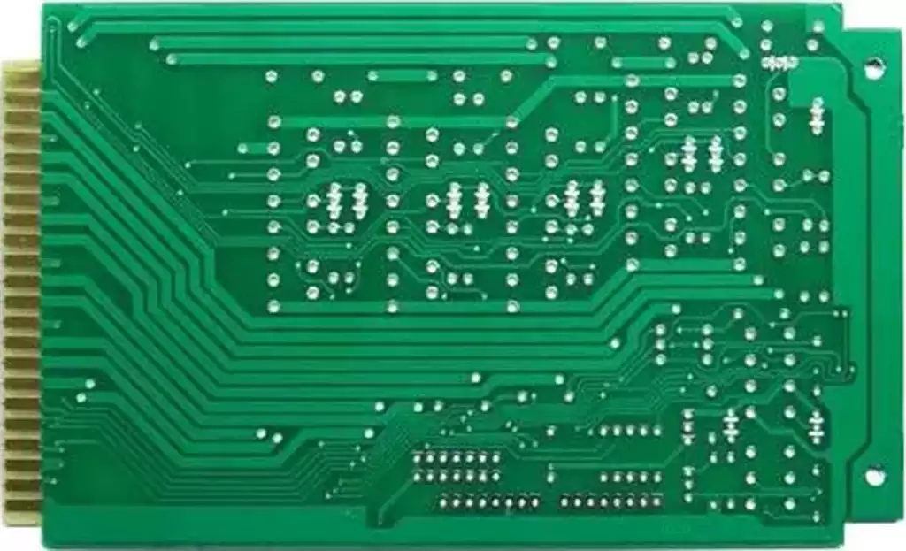
A bare circuit board, i.e. a printed circuit board without any processing, protective coverings or assembly of components, exists in its minimalist form as an electronic circuit connector. In short, it is a printed circuit board without electrical properties.
Bare board circuit board according to its construction characteristics, can be divided into single panel, double-sided board and multilayer board three types:
Single-sided boards, as the name implies, have only one side covered with copper, and that side is chemically etched. Because it is suitable for simple circuits, manufacturing costs are relatively low.
Double-sided board is manifested as two sides are not affected by the connecting lines, suitable for more complex circuit layout, but the corresponding manufacturing costs will also be enhanced.
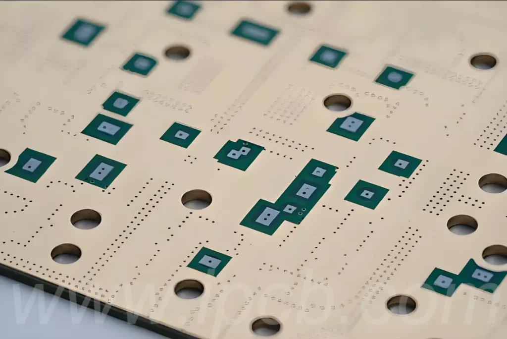
Multilayer boards are made by pressing multiple single or double-sided boards together, usually containing more than four layers. Multilayer boards not only have more complex circuit layouts, but also allow for smaller volumes, but are more expensive than single and double-sided boards.
The manufacturing process for bare board circuit boards involves a number of steps:
First of all, the pre-preparation is essential, including raw material inspection, circuit design, software mastery and so on. Then comes the production of the inner layer board, which is obtained by cutting and laminating copper foil. Then comes the pattern exposure, which can be done by photocopying or etching method, etc. The etching session then removes the unwanted metal to form the basic shape. This is followed by operations such as double-sided bonding and pressing of the outer laminate. The surface covering segment then gives the board anti-corrosion and printing features by spraying and printing. After high-temperature drying is completed, performance checks are performed to ensure proper functioning.
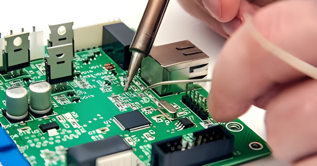
There are also some points to note when working with Bare PCB. First, since the BPCB does not have any protective layer, physical and electrical isolation measures need to be taken to prevent damage. Second, the design needs to take into account the wiring and electrical characteristics, as well as the physical and mechanical connections. Furthermore, the lack of conductivity will affect the operation of the board, and special attention needs to be paid to the conductivity problem. In addition, Bare PCB manufacturing requires a certain level of technology and equipment support, should be purchased from the regular manufacturer, and in the design process to take into account the aesthetics and safety. Finally, with increasingly stringent environmental regulations, the choice of BPCB need to draw on experience to ensure compliance.
Bare circuit board, as a basic form of circuit board, have the advantage of low-cost preservation. However, they also need to be handled carefully in use to ensure their safety and effectiveness.