Rogers PCB Electromagnetic Compatibility
The stability of the dielectric constant (Dk) is central to the electromagnetic compatibility (EMC) of Rogers PCBs and represents the most significant distinction between them and standard FR-4 PCBs. Many
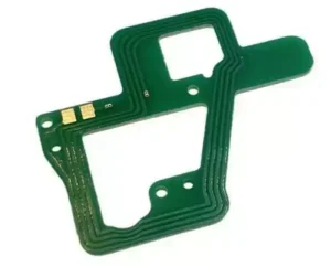
Methods for controlling FPC impedance
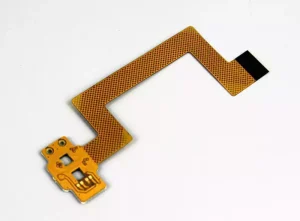
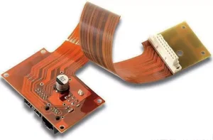
The impedance of an FPC (flexible printed circuit) refers to the electrical resistance encountered by a signal as it travels along the circuit; it is a key indicator of signal
Factors affecting FPC pricing
FPC quotations are influenced by a combination of four key factors: materials, structural design, manufacturing requirements and order volume. Any variation in the selection or specifications of these elements will
The Engineering Physics of FR4 PCB Thickness and Impedance Control
The Physical Nature and Standard Evolution of FR4 pcb Thickness In the field of printed circuit board (PCB) manufacturing, FR4 (Flame Retardant Rating 4) is not only a material but
The protective role of coverlay on FPCs
The coverlay serves as the core flexible insulating protective layer for FPCs. Consisting of a PI film substrate combined with a specialised adhesive layer, it provides insulation, reinforcement and coverlay
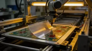
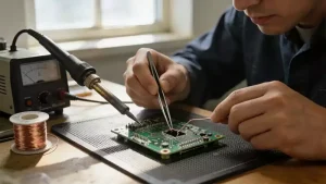
Rogers PCB High-Frequency Soldering Process
In the manufacture of RF and microwave circuits, Rogers PCBs serve as the core substrate due to their low dielectric loss and high dielectric stability. As the critical process for
Rogers PCB Transmission Line Selection
In high-frequency circuit design, Rogers PCBs have long been recognised as the industry standard thanks to their outstanding performance. With their stable dielectric properties and low-loss characteristics, they are virtually
Design of the Rogers hybrid laminates
Rogers material is the material of choice for high-frequency applications due to its excellent dielectric properties, but its high cost limits its widespread use; FR4 material offers outstanding value for
The reasons for the high temperature resistance and long service life of RO4835
The extended service life of RO4835 at high temperatures stems from the systematic synergy between its material formulation, structural design and process optimisation. In harsh high-temperature environments such as outdoor
Rogers PCBs: Dual Advantages of Thermal Stability and Reliability
As a benchmark product in the field of specialised high-frequency substrates, the thermal stability and reliability of Rogers PCBs directly determine the performance and service life of equipment in high-end
The dielectric constant is crucial in the design and manufacture of high frequency PCB
The dielectric constant, also known as the permittivity, is a key electrical parameter that measures a material’s ability to store electrical energy in an electric field; it essentially reflects the
A Comparison of FR-4, Aluminium Substrates and Flexible Printed Circuit Boards
FR-4, aluminium substrates and flexible printed circuit boards are the three most common PCB material options in electronic design. This article compares them across four dimensions—material properties, performance differences, manufacturing
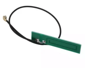
A Comparison of PCB Antennas and FPC Antennas
The choice of antenna directly impacts a device’s communication performance and structural design. This article compares the key differences between PCB antennas and FPC antennas across four dimensions—structure and materials,
How to prevent ink from peeling off the surface of PTFE substrate
Due to their extremely low surface energy and high chemical inertness, achieving reliable ink adhesion on PTFE substrates has long been a key challenge in the manufacturing process. To ensure
Micro-perforation process for PTFE substrates
PTFE substrates have become a key material in high-frequency, high-speed PCB applications such as 5G communications and millimetre-wave radar, owing to their extremely low dielectric constant and dielectric loss. Micro-drilling
PTFE PCB high-frequency routing
Unlike traditional substrates such as FR-4, PTFE PCBs have a dielectric constant (Dk) that remains stable between 2.0 and 2.6, with a dielectric loss factor (Df) as low as 0.0005–0.002.
Applications and Characteristics of PTFE PCBs in High-Frequency Circuits
PTFE PCBs are high-frequency printed circuit boards that use polytetrafluoroethylene (PTFE, commonly known as ‘Teflon’) as the dielectric substrate. Unlike traditional FR-4 epoxy resin materials, PTFE is a fluorinated polymer
Impedance Control in 4 Layer Boards
The impedance stability of high frequency 4 layer board is a key factor determining the quality of signal transmission in electronic devices. Solder mask application and surface treatment, as core
Causes of Warpage in Asymmetric 4 Layer PCB Stacking Designs and Countermeasures
As a widely used type of multilayer board in electronic devices, the standard symmetrical stack-up design for 4 layer PCBs typically employs a symmetrical structure of ‘signal layer – power
A comparison of 2 layer pcb and 4 layer board
In the design and manufacture of printed circuit boards, the choice of layer count is never merely a numbers game—it directly affects the circuit’s electrical performance, immunity to interference and
Repairing broken PCB circuit board traces
In the PCB manufacturing industry, broken circuit board traces are a recurring challenge at every stage, from production and testing through to transport and subsequent use. The causes are varied—they
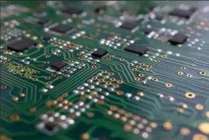
High frequency PCB via optimisation
The success or failure of signal transmission in high frequency PCBs is often determined by details imperceptible to the naked eye. Via holes, serving as the core conduits for interconnecting
Interpretation of Antenna PCB Return Loss Curves
Return loss serves as a pivotal metric for evaluating the signal transmission efficiency of antenna PCBs. It quantifies the ratio of power reflected back to the source due to factors
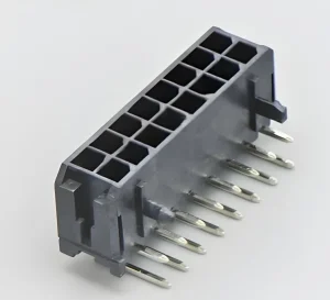
Understanding PCB Socket Pins and Their Role in Reliable Electronic Connections
The Fundamental Role of PCB Socket Pins in Electronic Connections In the design and assembly of electronic circuits, PCB socket pins are a crucial component for achieving electrical connections. They