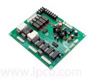
Flow of custom pcba
Custom PCBA refers to the customised design and production of PCBA products according to customer requirements. This includes selecting the right components for the specific application, designing a board layout
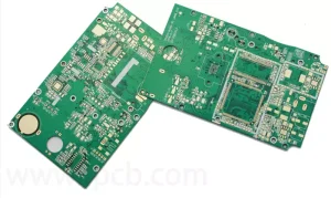
Difference between high frequency PCB and high speed PCB
High frequency pcb and high speed pcb belong to the same PCB circuit boards used for signal transmission, however, there are significant differences between the two in the actual application
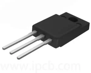
Moisture Sensitive Level and Components Applications
The MSL (Moisture Sensitive Level) standard is a classification system used by the electronics industry to assess the sensitivity of components to moisture, which classifies components into eight different levels
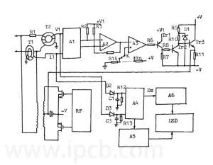
RF Circuit Design Principles and Key Points
The fundamentals of RF circuit design include: RF Circuit Layout PrinciplesWhen designing an RF layout, priority must be given to meeting the following general principles: (1) As far as possible

Principle and Prevention of Pillow Effect on Solder Joints
Solder Joint Pillow, also known as the pillow effect (Head-in-Pillow, HIP), is an undesirable phenomenon in which the solder balls of BGAs, CSPs and other components fail to fully fuse
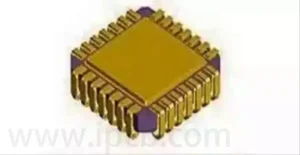
Chip Packaging Process Flow
As a key necessary step in the integrated circuit manufacturing process, chip packaging and testing plays a vital role. Specifically, this link will carry out a series of fine operations

Key technologies of camera circuit boards
With the rapid development of science and technology, the impact of digital imaging technology in our lives is becoming more and more profound. From daily smartphones and tablets to high-precision
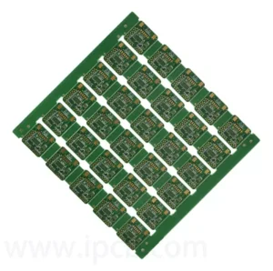
BGA PCB design and wiring
BGA Test Fixture (Ball Grid Array Test Fixture) is a test tool for testing BGA chips, which can provide electrical test, signal acquisition and programming functions for the chip. In
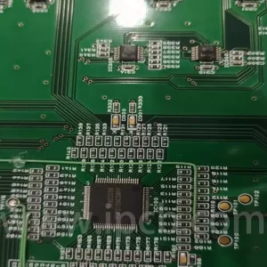
Functions and applications of potentiometer circuit board
A potentiometer circuit board is an analogue circuit element used in electronic circuits, usually to adjust the resistance of a circuit in order to control its performance and function. It
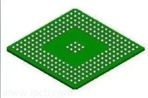
Significance of BGA welding ball diameter tolerance
BGA pad diameter tolerance, that is, the maximum allowable deviation range of the diameter of the ball grid array package pad. In the manufacturing process of electronic components, the control
Flame retardant properties of circuit board
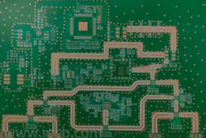
Circuit boards are classified according to their self-extinguishing time after fire ignition, and are usually classified into three grades: UL94 V-0, UL94 V-1, and UL94 V-2. The evaluation of the
Remote control circuit board technology
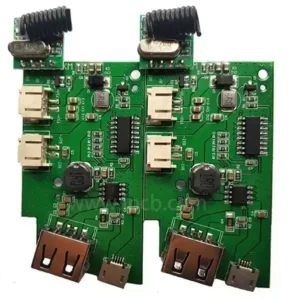
A remote control circuit board is an electronic device used to remotely control equipment. It is based on wireless communication technology and uses wireless signal transmission between the transmitter and
High Voltage PCB Design Essentials
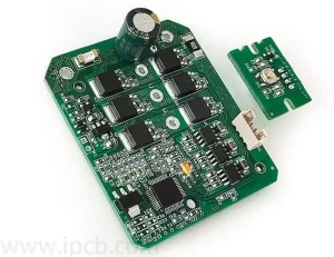
High voltage pcb is circuit board that can withstand high voltages and are commonly used in high-voltage electronic equipment. It must not only be able to withstand high voltages, but
FPC soldering technology
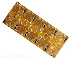
Flexible Printed Circuits (FPC) as electronic equipment thin and highly integrated core carrier, its welding technology directly affects product performance and reliability. Common soldering methods for flexible circuit boards:Thermocompression SolderingThermocompression
Hard Drive PCB Board Functions and Failures
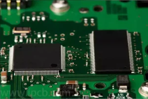
The hard drive pcb board acts as a bridge between the internal hard drive and the motherboard of the computer, and its role is to convert the electrical signals received
Why does the fpc smt process need fixture
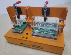
Why FPC SMT must use the fixture, FPC flexible board has a unique physical characteristics, so it can not be directly applied to the standardised SMT (surface mount technology) production
FPC Plating and Plating Selection Details
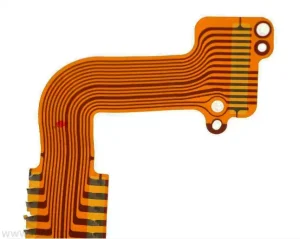
Plating is an extremely critical step in the FPC manufacturing process. Plating not only strengthens the circuit’s conductivity, but also improves its corrosion resistance and appearance. FPC (Flexible Printed Circuit)
Circuit board aging
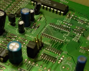
Circuit board aging refers to the natural phenomenon of gradual changes in the properties, structure and performance of circuit board materials after long-term use of electronic equipment. The effects of
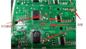
Continuous tin industry causes and solutions
What is continuous tin? Continuous tin refers to the soldering of circuit board pads on the solder joints after the emergence of two and more solder joints. Pins of the
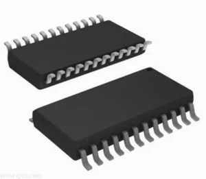
The role and application of power ic chip
A power ic chip is a type of integrated circuit chip that is mainly used to control and manage functions such as power supply and protection. They are usually used
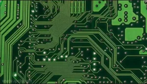
Relationship between printed circuit boards and ic
Printed Circuit Board as a key component in the field of electronics, the principle of its work is in the conductive substrate precision etching or printing ‘circuit layout pattern’, as
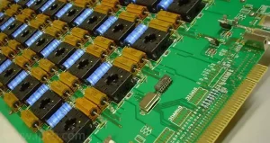
Circuit Board burn in Test
Burn in test is the process of running a circuit board or equipment for an extended period of time under tightly controlled environmental conditions to simulate actual circuit board usage
Purpose and method of pcb inspection
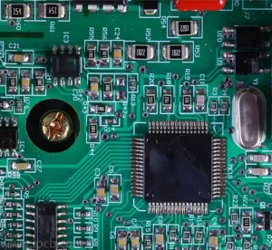
PCB Inspection is a comprehensive inspection of a printed circuit board that includes cosmetic, dimensional, solder joint, component mounting, electrical and functional testing. These steps ensure that the PCB is
Role of Automatic Test Equipment
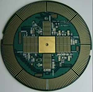
Semiconductor test boards, or ATE (Automatic Test Equipment) as we often call them, are an essential part of the semiconductor industry. Semiconductor test boards are specialised circuit boards used to