PCB lamination process
PCB lamination is a key process step in the manufacture of multilayer printed circuit boards (PCBs). In this process, multiple thin, pre-processed circuit board layers (including copper foils, insulating substrates,
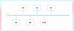
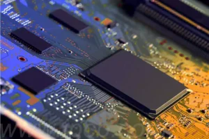
Capacitors And Resistor Enhanced EMS and ESD Protection
Agnetic environments and the control of interference with other equipment. ESD protection is the key to ensure that the equipment is not damaged in the electrostatic environment. This article will
PCB anti static electricity design
Static electricity arises from the separation of charges that occurs when two different materials come into contact with each other or are rubbed together, causing an object to become electrically
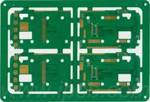
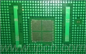
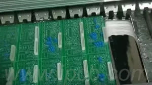
PCB panelization technology analysis
What is pcb panelization?PCB panelization refers to the process of integrating several small PCB boards into one large board by the manufacturer. From the initial stage of PCB design until
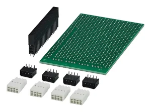
Overview and Application Analysis of Perf Board
Perforated sheet, as an important industrial material, is widely used in many fields such as construction, electronics, machinery and so on. It is characterized by having evenly distributed holes on
PCB Warpage Repair Method
In the PCB manufacturing process, pcb warpage problem has been one of the key factors affecting product quality and productivity. Warped PCB boards are not only difficult to subsequent assembly
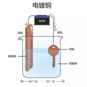
CIrcuit board Side Plating Technology
Circuit board side plating, also known as edge copper plating, refers to copper plating applied to at least one of the side edges of a PCB board that extends from
PCB Copper Layup Technology Enhances PCB Board Performance
PCB Copper Layup is the process of filling areas of a PCB board that are not wired or unused spaces with solid copper skins. Copper plays multiple key roles in

Application and Development of Fusible PCB
In the electronics manufacturing industry, fusible PCB, as a special type of printed circuit board, has gradually attracted market attention in recent years. As electronic products develop towards high integration,
PCB design board pitch optimisation
On a printed circuit board,board pitch refers to the distance between two pins or components,which is usually measured in millimetres. The correct layout of components is essential in the design
PCB board beveling technology
What is beveler in pcb?The PCB beveling machine is a specialised equipment for chamfering the edges of circuit boards.Beveling of circuit boards refers to a special treatment on the edges
Wave soldering dross problems and countermeasures
In the electronics manufacturing industry,wave soldering, as an important connection technology, is widely used in the assembly process of circuit boards. However, in practice, excessive tin impurities and the generation
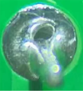
Reasons and solutions for PCB tin explosion phenomenon
The phenomenon of PCB tin explosion refers to the occurrence of tin explosion and ejection at the junction of solder joints and soldering materials during the soldering process of PCB
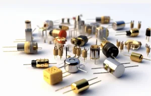
Analysis of the Basics and Applications of Circuit Components
Circuit elements play a vital role in the development of electronic technology. They are the basic components of circuits, and the normal operation of various electronic devices is inseparable from
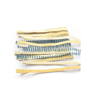
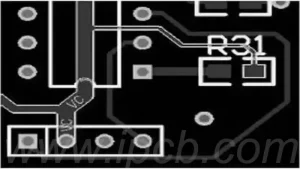
Resistance Matching Principles and Applications in PCB
In electronic circuit design, resistance matching is a basic but crucial concept. Whether it is a high-frequency communication system, a sensor network, or a power amplifier circuit, the rationality of
Optimisation of pcba processing costs
In the fierce competition in the electronics manufacturing industry, effective control of PCBA (Printed Circuit Board Assembly) processing costs is the key to enhancing the competitiveness of enterprises. From board
Properties and Applications of Alumina Board
Alumina board,the main component of which is aluminium oxide (Al₂O₃), is a ceramic material made by high temperature sintering. With its excellent physicochemical properties,it shows a strong potential for application
PCB solder blow hole defects and solution
Solder blow hole refers to the plug-in over the wave soldering, the hole in the gas due to high temperature and out of the solder, so that the hollow formed
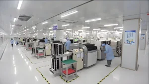
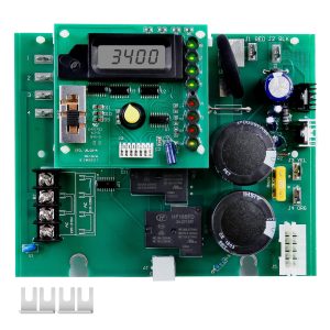
Importance of PCBA Function Tester
In the modern electronics manufacturing industry, it is crucial to ensure the quality and performance of circuit boards. With the development of science and technology, the complexity of electronic products
Critical Role of Circuit Board Spacers and Material Selection
The circuit board spacers are key components in the connection between the circuit board and its components.Often placed at the bottom of the board’s component pads, they provide cushioning and
What is Cold Welding in the Electronics Industry
Cold welding is a special method in welding technology, which is widely used in metal processing, electronic manufacturing and the production of high-precision equipment. What is cold welding in the

Circuit board Labels
Circuit board Labels,Printed circuit boards (PCBs) are at the heart of most electronic products, including computers, printers, home entertainment devices, “smart” kitchen appliances and mobile phones.Labeling PCBsTo ensure long-term traceability
PCB solder pad came off Guide
PCB solder pad came off refers to the phenomenon that the solder pad is separated from the printed circuit board. The solder pad is a conductive graphic on the PCB
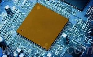
glx pcb main
Definition of glx pcb mainglx pcb main is a main circuit board designed for the core of electronic devices. It is the central control unit of the system, responsible for