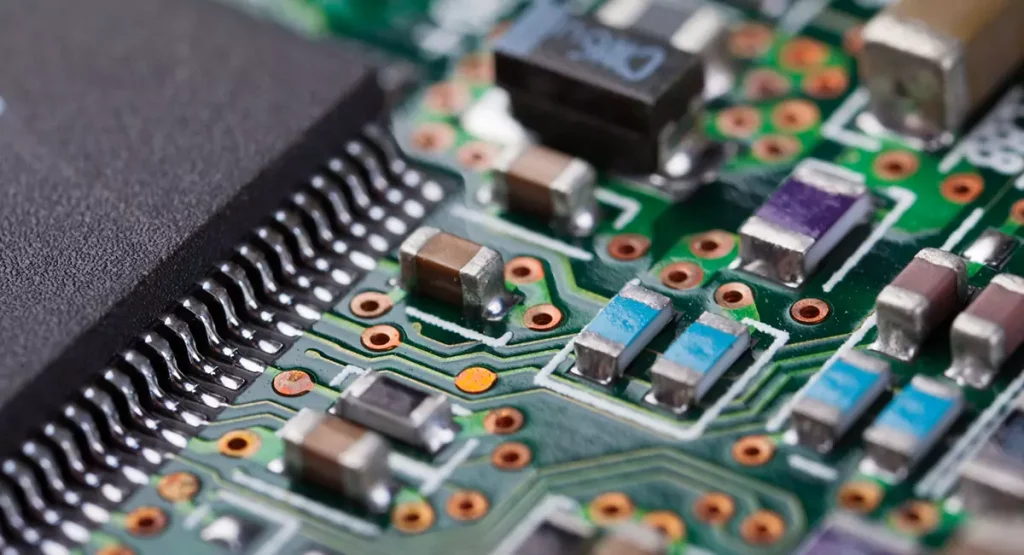
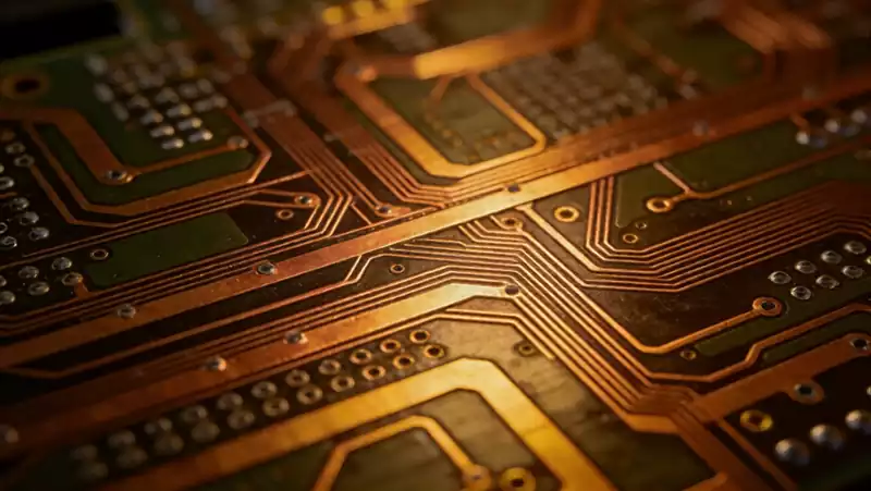
A bluetooth player circuit board must convert a wireless audio stream into stable speaker output without adding noise, distortion or connection problems. Although the board may appear compact, the signal passes through several different electrical environments before any sound is produced.
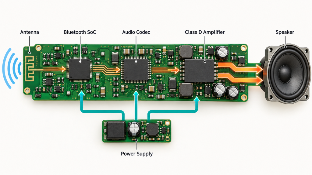
A reliable bluetooth player circuit board depends on the interaction between its antenna, Bluetooth SoC, audio codec, amplifier and power supply. A weakness at one stage can appear elsewhere as short wireless range, background noise, weak bass or distorted output.
Pairing Establishes the Wireless Audio Link
Audio playback begins when the player discovers and connects to a phone, computer or other source. For conventional Bluetooth audio products, the Advanced Audio Distribution Profile defines the requirements for high-quality audio distribution between compatible devices. Newer Bluetooth LE Audio products use a different architecture, so the firmware and hardware must support the intended audio profile.
On a bluetooth player circuit board, pairing is controlled primarily by the Bluetooth SoC and its firmware. However, unreliable pairing is not always a software problem. Antenna placement, power noise and incorrect RF matching components can reduce connection stability before audio processing even begins.
The Antenna Feeds the Bluetooth SoC
The antenna receives a very low-power RF signal, making this area sensitive to nearby copper, batteries, speaker magnets and metal enclosures. A correctly routed board can still lose wireless range when the finished product places a cable or battery directly beside the antenna.
For this reason, the antenna section of a bluetooth player circuit board normally requires a defined copper keep-out area and controlled spacing from surrounding mechanical parts. The enclosure should be included in wireless testing because open-board measurements do not represent the final product.
Once received, the wireless signal enters the Bluetooth SoC. The device manages the radio connection, extracts the audio stream and converts the compressed data into digital audio samples.
Audio Data Remains Digital After Reception
The output from the Bluetooth SoC is commonly transferred through a digital audio interface to an external codec or amplifier. Some products integrate more of this processing inside one device, but the functional sequence remains similar.
At this point, a bluetooth player circuit board is handling clocked digital data rather than an analog music waveform. Incorrect clock configuration, firmware settings or digital interface timing may produce silence, intermittent playback or channel errors even when pairing appears normal.
The Digital to Analog Handoff Determines Audio Quality
The audio codec converts digital samples into an analog signal that can be amplified. This handoff is especially sensitive because digital switching noise, power-supply ripple and ground voltage changes can enter the low-level analog path.
Component placement around the codec therefore affects audible performance. Decoupling capacitors need short connections to the relevant supply pins, while analog traces should be kept away from RF clocks and high-current amplifier outputs. A continuous return path is usually more important than visually separating the board into disconnected ground areas.
The audio section of a bluetooth player circuit board should also avoid routing low-level signals alongside switching regulators. Even when the regulator operates above the audible range, its harmonics and load transients can enter the codec supply or analog ground. The resulting fault may be heard as hiss, buzzing or a tone that changes with wireless activity.
These problems are difficult to identify through ordinary continuity testing because every connection may still be electrically correct. Noise measurements and listening tests must be performed while the radio, processor and amplifier are operating together.
The Amplifier Changes the Electrical Environment
After digital-to-analog conversion, the signal enters the power amplifier. Portable Bluetooth products frequently use a Class D amplifier because it provides efficient speaker drive with relatively low heat generation.
The amplifier is where a bluetooth player circuit board changes from small-signal processing to high-current switching. Speaker current, power-supply current and switching return paths must remain compact. Otherwise, the amplifier can inject noise into the codec or radiate interference toward the antenna.
Output traces should be routed as a controlled pair and kept away from the RF section. Bulk capacitance supports low-frequency current demand, while local ceramic capacitors handle fast switching edges. Texas Instruments’ Class D layout guidance similarly emphasizes close power decoupling and careful placement of output filtering components when they are required for EMI control.
Poor thermal-pad soldering can create another hidden problem. The amplifier may pass a short functional test but overheat during sustained high-volume playback. X-ray inspection is useful when the thermal pad is located beneath the package and cannot be evaluated by AOI.
One Input Supply Creates Several Power Domains
A battery or DC adapter may feed the entire product, but the radio, digital processor, codec and power amplifier do not have identical supply requirements.
Inside a bluetooth player circuit board, the amplifier creates the largest current changes, while the codec requires a comparatively quiet supply. Supply filtering, regulator selection and return-path control prevent amplifier load changes from modulating the RF and analog sections.
Assembly Defects Often Appear as Audio Symptoms
Manufacturing variation can affect the signal path even when the PCB design is correct. An incorrect RF matching capacitor can reduce range, insufficient solder beneath the amplifier can increase temperature, and contamination around the codec can create leakage or noise.
This makes process control important for every bluetooth player circuit board entering production. Component verification, solder-paste inspection, AOI and X-ray should be combined with functional audio testing rather than treated as separate quality activities.
Functional Testing Must Follow the Complete Path
A useful test does more than confirm that the board powers on. The bluetooth player circuit board should pair with a reference source, reconnect after a power cycle and play a known audio file through every output channel.
Testing should also check idle noise, left and right channel operation, output level and distortion at realistic volume. High-volume playback is particularly valuable because it exposes supply droop, weak solder joints and thermal protection that may remain hidden at low power.
For a bluetooth player circuit board entering production, iPCB can combine PCBA inspection, firmware programming, wireless connection checks and audio output testing within one controlled manufacturing process. This provides better fault isolation than testing the assembled product only after enclosure installation.
Every Stage Must Preserve the Audio Signal
Reliable wireless playback is not created by the Bluetooth chip alone. The complete path must preserve signal integrity from the antenna and Bluetooth SoC through the audio codec, Class D amplifier and speaker connection.
When RF placement, quiet analog power, high-current routing and end-to-end testing are controlled together, a bluetooth player circuit board can maintain stable pairing and consistent sound quality across the entire production batch.