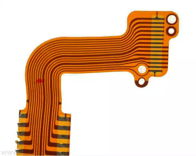
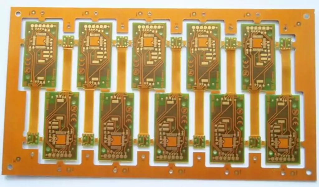
In the printed circuit board (PCB) design process,body to body clearance for smt parts refers to the physical distance between different surface mount components (such as resistors, capacitors, chips, etc.).Ensuring proper clearance between these components is critical,as it not only relates to the reliability and performance of the circuit, but also has a direct impact on the manufacturability of the entire PCB process.
Factors affecting the body-to-body clearance for smt parts in PCB design
1.Signal integrity
PCB design, the body to body gap for signal integrity has an important impact.If the gap is too small,high-frequency signals may be degraded due to electromagnetic interference (EMI),thus affecting the performance of the circuit.For example,interruptions in the signal return path may increase radiated noise and make the signal unreliable.Therefore,special attention needs to be paid to signal wiring and spacing during design to avoid signal interference.
2.Thermal Management
Body-to-body clearance for smt parts also directly affects thermal performance.As the power of electronic components increases,if the gap is too small,it will result in the heat not being able to be effectively distributed,which may cause the device to overheat,thus reducing its performance and life.A good gap design can improve heat dissipation efficiency and prevent localized overheating.
3.Material properties
Material properties such as dielectric constant and dielectric strength are also very critical in PCB design.A high dielectric constant may affect the impedance and capacitance of the circuit,which in turn affects the integrity of the signal.Dielectric strength determines the maximum electric field strength that the PCB can withstand,ensuring that the circuit will not break down at high voltages.
4.Environmental Factors
The impact of environmental factors on the gap should not be ignored.For example,changes in humidity may lead to expansion or contraction of the PCB material,thus affecting the body to body clearance for smt parts and overall stability.Changes in temperature may also cause thermal expansion,changing the physical dimensions of the gap.These environmental factors need to be taken into account during design to ensure the stability and reliability of the design.
5.Processing accuracy
The processing accuracy of PCBs directly affects the body to body clearance for smt parts.In the manufacturing process,tool wear and changes in material properties may lead to the actual gap does not match the design.Therefore,a reasonable machining process and strict quality control are essential to maintain the accuracy required by the design.It is recommended to maintain a certain safety clearance during design to accommodate the effects of machining errors.
Effects of too small a gap between SMT components
Too little clearance between SMT (surface mount technology) components can lead to a variety of problems,the most notable of which include heat buildup and signal interference.When there is insufficient clearance,heat cannot be dissipated effectively between electronic components,which can cause thermal stress and potentially lead to component failure or performance degradation.In addition,too small a gap can cause electrical isolation problems,increasing the risk of short circuits and crosstalk,which can affect the signal integrity of the circuit and the overall reliability of the device.
2.Generation of soldering defects
Narrow component gaps can also lead to soldering defects, such as bridging and inadequate solder joints. These problems can lead to poor electrical connections, increasing the risk of component failure and can cause potential short circuits, which can affect the performance and reliability of the overall product. This situation is particularly important in the SMT assembly process, as the quality of the soldering is directly related to the final result of the product.
3.Assembly Process Challenges
Insufficient clearance between components can also lead to a number of challenges during the assembly process. For example, solder paste may bridge or flow insufficiently during soldering, which can ultimately lead to a weak connection. Ensuring proper clearance is therefore not only critical to the soldering process, but is also the basis for overall assembly quality assurance.

Reasonable design body to body clearance for smt parts method
- Consider component size factors
When designing the body to body clearance for smt parts,the dimensions of individual components need to be carefully considered first. Usually, the spacing between components should be at least 1/4 to 1/2 of the electronic component body size to ensure good soldering and heat dissipation conditions. - Soldering process requirements
Different welding processes have different spacing requirements. For example, the use of wave soldering, components need to leave enough space between the welding operation. Therefore, the design needs to fully understand the welding process used, and according to its requirements to adjust the corresponding gap. - Electrical performance considerations
When designing the spacing, the electrical performance must also be taken into account. Some of the pins may affect the signal quality due to electromagnetic interference, so it is necessary to set a certain distance to reduce such interference. This spacing usually depends on the strength of the interference source and the sensitivity of the affected component. - Influence of cabling design
In order to ensure the reliability and stability of the circuit board, the wiring design will also affect the spacing between components. Too dense wiring can lead to signal interference and heat dissipation problems, so it is necessary to rationalize the location of components and wiring. - Evaluation of manufacturing cost
Under the premise of ensuring the function and performance, the design also needs to consider the manufacturing cost. A smaller pitch can reduce the size of the board, thereby reducing costs, but too small a pitch will also increase the difficulty and risk of manufacturing, so the pros and cons should be weighed.
In the printed circuit board (PCB) design process, a reasonable body to body clearance for smt parts design is critical. It not only directly affects signal integrity and thermal management, but also relates to material properties, environmental adaptability and processing accuracy. In order to avoid the many problems brought about by too small a gap, such as heat buildup, signal interference and soldering defects, design engineers need to comprehensively consider factors such as component size, soldering process, electrical performance and manufacturing costs. In the future of PCB design, focusing on the rational layout of components will enhance product performance and reliability, and ensure that electronic devices in the increasingly complex application environment, stable operation. By continuously optimizing our design strategies, we can better meet the needs of high-performance electronic products.