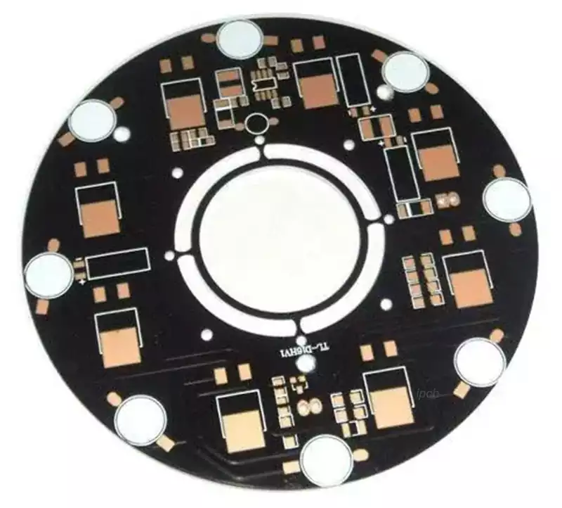
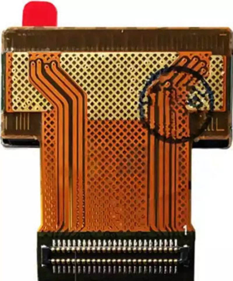
Camera pcb boards, or Camera circuit boards, are printed circuit boards specifically designed for on-board cameras, forming the fundamental structure of digital imaging equipment.
Cameras are complex electronic devices comprising multiple components, with the camera pcb board being one of their vital constituents. Also termed the camera pcb board, the camera mainboard serves as one of the core internal components, housing vital elements such as the processor, memory, interface chips, and sensor control chips. It performs functions including data processing and signal conversion, enabling the camera to deliver enhanced processing capabilities and comprehensive control functionality.
Functions of the Camera PCB Board
- Operational Control: The camera pcb board manages communication and operation between internal components via the processor, ensuring the camera functions correctly.
- Image Processing: The processor and sensor controller on the mainboard perform operations such as noise reduction, autofocus, colour balancing, and post-processing on raw images captured by the sensor, enhancing photographic outcomes.
- Storage Management: Storage management chips on the mainboard control the camera’s internal memory, facilitating the storage and retrieval of photographs and video files.
- Data Transmission: Interface chips on the camera’s mainboard facilitate data transfer, communication, and interconnection between the camera and external devices such as computers or mobile phones, enabling the transmission and sharing of photo and video files.
- Power Management: Power controllers on the camera’s mainboard efficiently regulate electrical supply to internal components, extending battery life and enhancing operational efficiency.
Key Design and Layout Considerations for Camera PCB Boards
The performance of a camera circuit board directly determines the final imaging quality. An excellent design minimises noise interference, ensures high-speed signal integrity, and guarantees stable system operation in complex electromagnetic environments. Neglecting these details may result in image issues such as noise, banding, or colour distortion. Therefore, adherence to strict design principles is paramount.
Core Considerations in Camera PCB Board Design:
- Power Integrity and Decoupling Capacitor Placement
The camera’s image sensor and processor are highly sensitive to power supply purity. Power noise directly couples into the image signal, manifesting as visible interference. Therefore, all power rails—including AVDD (analogue power), DOVDD (digital I/O power), and DVDD (core digital power)—must be adequately filtered and decoupled. Decoupling capacitors (typically 100nF) must be placed as close as possible to the chip’s power pins to provide a low-impedance path for transient currents and filter out high-frequency noise. - High-Speed Signal Integrity
Interfaces such as MIPI and LVDS within camera modules carry high-speed image data. The routing of these differential signal pairs must strictly adhere to impedance control requirements (typically 100 ohms or 90 ohms). Traces should be kept equal in length, parallel, and with minimal use of vias. Where layer changes are necessary, a return ground via must be placed adjacent to the differential via to provide a continuous return path for the signal, preventing impedance discontinuities and signal reflections. - Electromagnetic Compatibility (EMC) Design
EMC design aims to reduce a circuit board’s external electromagnetic radiation while enhancing its resistance to external interference. Key measures include:
Ground plane integrity: Employing a complete, large-area ground plane as a signal return path to effectively shield against noise.
Signal Isolation: Physically separate high-speed digital signals, analogue signals, and clock signals to prevent cross-coupling. For instance, MIPI differential pairs should be isolated using ground planes.
Ground Fencing: Implement ground fencing around critical signal lines (e.g., clock lines) and periodically add ground vias to create a Faraday cage effect, suppressing radiation.
- Component Layout and Grounding Strategy
Rational component placement underpins successful design. Compactly arrange critical components—camera connectors, sensors, processors, and power management units—to minimise key signal paths. Separate analogue ground (AGND) and digital ground (DGND) or implement single-point grounding to prevent digital noise from contaminating sensitive analogue circuits. Additionally, position the camera layout away from high-power radiation sources like GSM antennas.
Core application areas for camera PCB boards include:
Consumer electronics: This is the most widely recognised application domain, encompassing smartphones, tablets, laptops, and drones. Within these devices, camera PCB boards typically employ flexible or rigid-flex designs to accommodate extremely compact spaces and intricate structures.
Security surveillance systems: From home IP cameras to city street CCTV, camera circuit boards form the core of real-time monitoring and recording. These applications demand high stability and reliability, enabling continuous operation under diverse environmental conditions.
Automotive electronics: Modern vehicles increasingly incorporate cameras for reversing views, 360-degree surround vision, journey recording, and Advanced Driver Assistance Systems (ADAS). Automotive-grade camera PCB boards must meet stringent reliability standards, withstanding extreme temperature fluctuations, vibration, and shock.
Industrial Automation and Machine Vision: On production lines, industrial cameras perform product inspection, dimensional measurement, and robotic guidance. These camera PCB boards require high frame rates, high resolution, and precise synchronisation capabilities to support high-speed, high-precision automated processes.
Medical Devices: Within healthcare, camera circuit boards are deployed in endoscopes, capsule endoscopes, and diverse diagnostic imaging equipment. These applications demand extreme miniaturisation, biocompatibility, and low power consumption, often necessitating advanced flexible or micro-PCB technologies.
Artificial Intelligence and Internet of Things (AIoT): With the advancement of AI vision technology, camera PCB boards in smart locks, smart home devices, and edge computing equipment not only handle image capture but also integrate AI processing capabilities to enable intelligent functions such as facial recognition and object detection.
Common Issues with Camera pcb boards and Their Solutions
- Camera fails to power on: First inspect the power circuitry, storage chip, processor, and interface chips on the mainboard to ensure they function and communicate correctly.
- Camera fails to capture images: Check the sensor controller, storage chip, and processor on the mainboard to confirm they operate normally and communicate with other components. Attempt resolution while ensuring all parameters remain within specifications.
- Poor image quality: Examine the processor and sensor controller on the camera’s mainboard to ensure they correctly process image data. Attempt to improve image quality by adjusting parameters such as ISO and shutter speed.
The intricate design of camera PCB boards is pivotal to imaging quality and device performance. By aligning with diverse sector requirements, adhering strictly to design specifications, and resolving common issues, we can drive continuous advancement in camera technology.