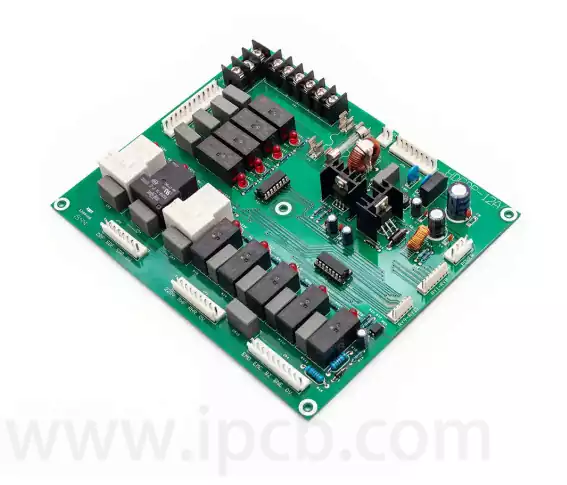
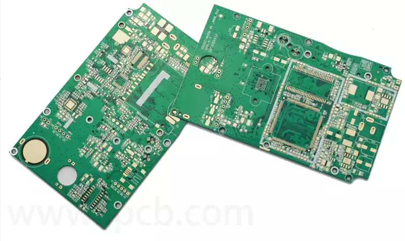
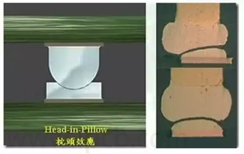
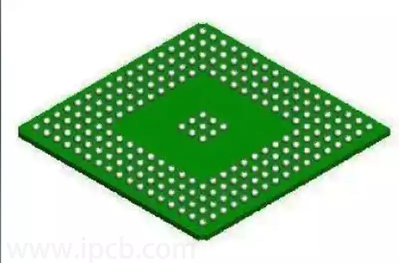
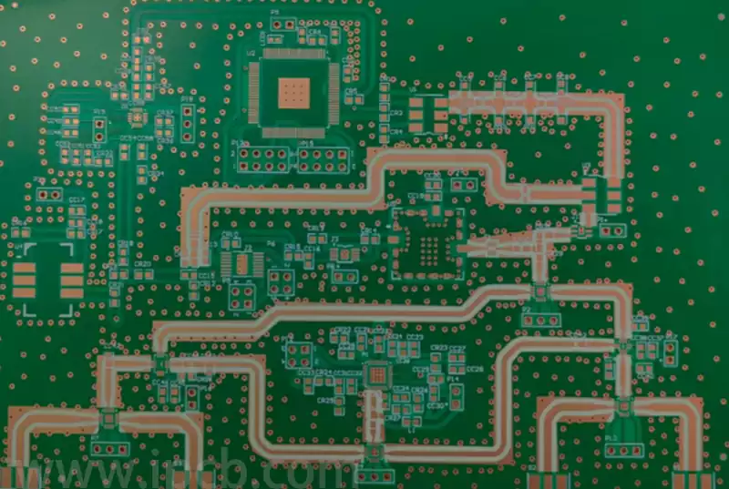
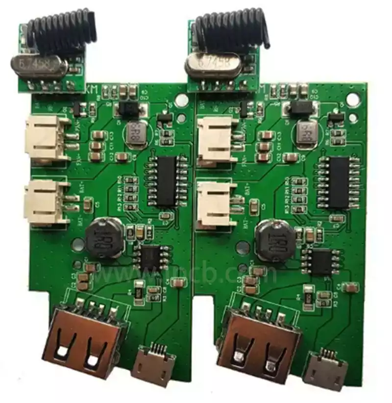
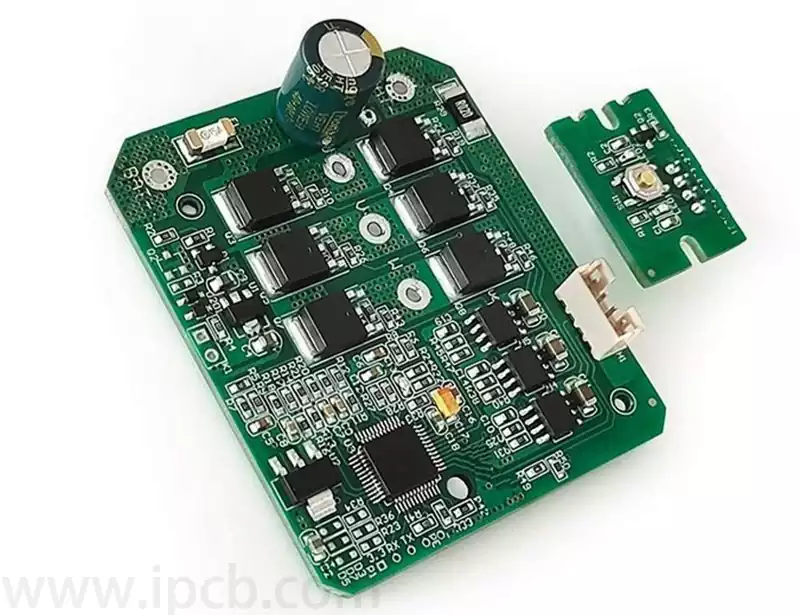
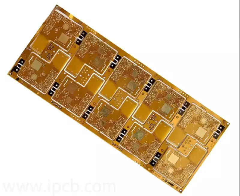
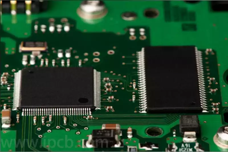
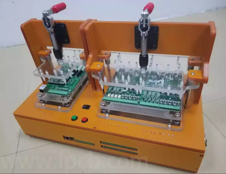
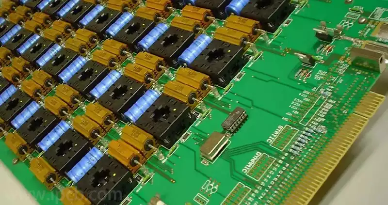
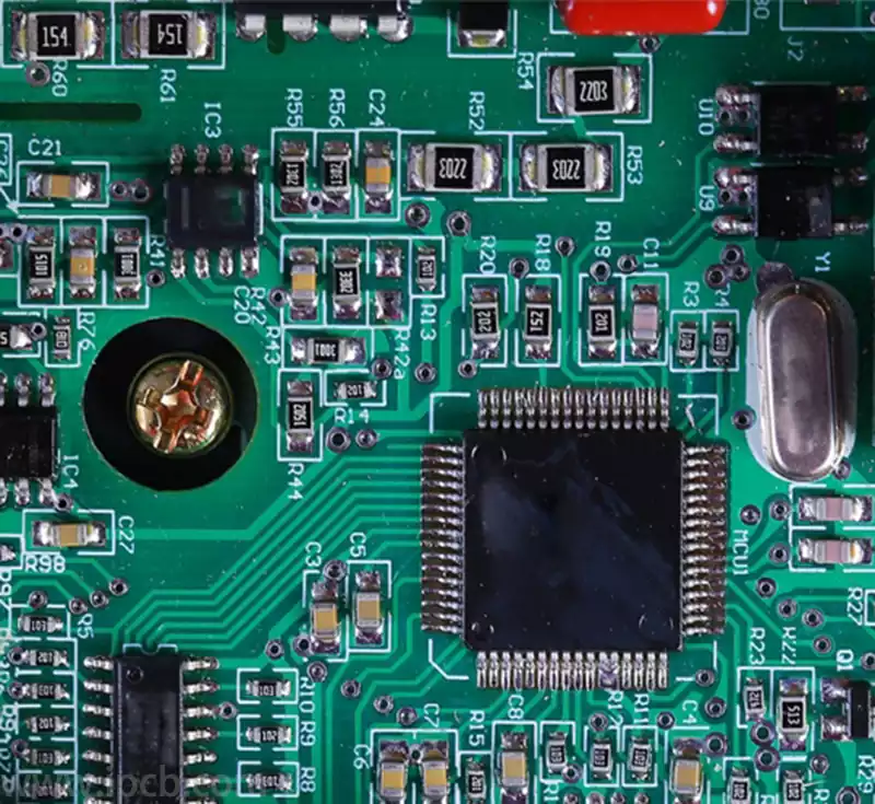
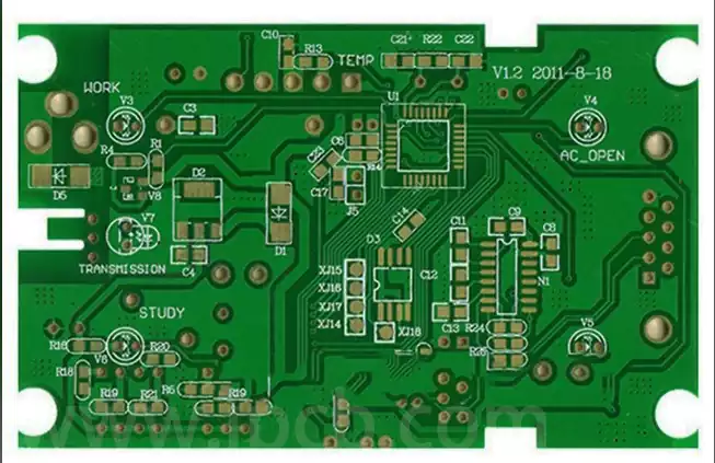
Technology Blog

warpage

Exploring Bare Board Warpage Problems and Their Solutions

Printed circuit board warpage refers to the phenomenon of PCB board bending, twisting or deformation during the working process. This warpage is usually caused by uneven heat distribution inside the circuit board. Warpage is the degree of bending of the PCB surface in different areas, and this performance parameter is very important in PCB design […]

bare-circuit-board

Bare circuit board: Manufacturing and Application Essentials

A bare circuit board, i.e. a printed circuit board without any processing, protective coverings or assembly of components, exists in its minimalist form as an electronic circuit connector. In short, it is a printed circuit board without electrical properties. Bare board circuit board according to its construction characteristics, can be divided into single panel, double-sided

ffc-vs-fpc

FFC vs FPC: Comparison and Selection of Flexible Connection

In the electronics industry, flexible connection technology has always been a key link, FFC vs FPC as two common flexible connection solutions, each with unique advantages and application scenarios. The difference between FFC vs FPC: Structure: FFC (Flat Flexible Cable) is a flat flexible cable, usually composed of metal foil and insulation, through the conductive

how-to-clean-a-pcb

PCB cleaning technology and quality assurance

PCB cleaning is an important processing procedure in SMT SMD processing, strictly in accordance with the requirements of the implementation can be removed in the electronic processing of some of the pollutants generated, such as flux, solder paste, adhesives, etc., a good cleaning process can protect the board in the use of the stability and

PCB mounting

PCB Mounting Holes: Key Elements for Design and Application

The pcb mounting holes are used to position or support the PCB for mounting. These holes are generally large and cover the external wiring, and can lead to incorrect mounting if not placed correctly. Basic Tips for Designing PCB Mounting HolesIn PCB design, the setting of mounting holes is an important part. EDA365 Electronics Forum

Fiducial-Marks

PCB Fiducial Marks: A Key Guideline for Manufacturing 

Printed Circuit Board fiducial marks are a reference point or identifier used to determine the relative position of other components or features on a PCB. These markers play a vital role in the manufacturing, testing, and assembly processes to ensure that components are accurately placed in the correct location for proper functioning of the circuit

PCB-Capacitors

PCB Capacitors: The Key to Circuit Efficiency

A PCB capacitor is an electronic component in which a capacitor is mounted directly onto a printed circuit board (PCB). It is mainly used to store charge and release it when needed to provide stable voltage and current, thus ensuring the normal operation of the circuit. Compared with traditional capacitors, printed circuit board capacitors have

PCB-density

PCB Density is Key to Electronics Manufacturing Enhancement

PCB density usually refers to the number of circuits, components and vias per unit area of the board. Higher density means more integrated functionality on the board, but also increased manufacturing difficulty and cost. Optimizing board density using multilayer PCB processing has become a widely used technology in the industry. Multilayer PCB processing involves carefully

chip-components

How to Soldering Chip Components on PCB Boards?

Soldering Procedures for Chip Components on PCBs: Soldering Process for SMD Components 1.Cleaning and securing the PCBBefore soldering the PCB, the first task is to ensure the cleanliness of the PCB boards. Any oily fingerprints and oxides must be removed to prevent negative effects on the soldering. When soldering PCBs manually, if conditions permit, a

PCB Manufacturing

PCB Manufacturing: The Importance of Test Point Setup

In the PCB manufacturing process, pcb test points, as a key element, play an important role in ensuring that circuit testing and debugging is carried out smoothly. Their existence not only enhances the reliability of the circuit, but also effectively reduces production costs and significantly improves manufacturing efficiency. The role of test points is broad

pcb-slip-ring

PCB Slip Ring:Unique Construction and Multiple Applications

PCB slip ring, as a highly efficient electrical transmission device, are widely used in scenarios that require continuous rotation while maintaining electrical connections.Compared to conventional slip rings, they feature a more compact and integrated design, enabling a brushless connection between the wires and the printed circuit board, thus ensuring the stability and reliability of power

FR4-relative-permittivity

FR4 relative permittivity and dielectric strength

FR4 material, as a commonly used glass fiber reinforced epoxy resin laminate material, occupies an important position in the electronics field due to its excellent electrical and mechanical properties. Among these properties, FR4 relative permittivity and dielectric strength are particularly critical, and together they determine the performance and application range of FR4 in circuit design.

screens printing

The process and importance of circuit board screen printing

Screen printing is the process of producing printed circuit boards using silkscreen printing technology. The screen printing layer is one of the layers used to label components or add other information when drawing PCBs. Through this printing method, the component shape, serial number and other descriptive text printed on the component surface or solder surface

ceramic-printed-circuit-board

Innovative applications for ceramic printed circuit board

Ceramic printed circuit board, which is manufactured on the basis of ceramic materials such as high-purity alumina ceramics, have become one of the highlights of modern electronics manufacturing. Compared to conventional plexiglass fiber circuit boards, ceramic circuit boards exhibit higher mechanical strength, excellent temperature resistance and thermal conductivity, as well as outstanding dimensional and chemical

how-to-cut-printed-circuit-board

How to cutting printed circuit board

Cutting printed circuit board is the process of dividing a whole or linked circuit board into two or several pieces according to a reasonable line. This step is carried out without affecting the effectiveness of the circuit board, which is conducive to the secondary processing and recycling of circuit boards for remanufacturing. Mechanical cutting of

single-sided-pcb

Single sided pcb: the cornerstone of electronics manufacture

A single sided pcb is a circuit board that has a copper-clad layer on one side only and no conductive layer on the other side. It relies on a layout such as open wires or common wires in order to realize the electrical connectivity of flat circuits. Compared to double-sided boards, single-sided boards are simpler

anti-pad

Functions and applications of circuit board anti-solder pads

A printed circuit board soldermask is a special construction designed to protect the integrity and stability of a circuit board by preventing solder from penetrating into areas of the board that should not be soldered during the soldering process. Soldermasks are typically placed on the substrate of a circuit board to cover a predetermined portion

potted-pcb

Potting PCB: Processes and Advantages in Depth

A potting pcb is a circuit board that has been subjected to a special potting process. This process usually involves the potting of a specific part of the board or the entire board surface with a protective insulating material. The potting material not only improves the mechanical strength of the board, but also effectively prevents

flex-PCB-bend-radius

Key elements and calculation method of flex PCB bend radius

Flexible PCB is carefully designed to cope with bending requirements, and their bend radius is a core parameter that ensures their functionality and durability. This parameter determines the extent to which the PCB can be bent safely without damage. The bending radius of a flexible PCB is influenced by a number of factors, the main

motherboard

In-depth analysis of computer motherboards

In 1936, Austrian Paul Eisler first utilized printed circuit boards in radios. By 1943, the technology was commonly used by Americans for military radios. And it was not until 1948 that U.S. officials officially approved the invention for commercial use. It was only from the mid-1950s that printed circuit boards came into widespread use. Before

wafer-testing

What is a Wafer testing?

Wafer testing is divided into two main categories: wafer testing (CP testing) and finished product testing (FT testing). Wafer testing is a moderate test of the capacitance and circuit function on each wafer after wafer fabrication is completed to ensure that its circuits are functioning properly before it is sent to the packaging plant for

hard-gold-pcb

Hard Gold PCB in Electronics Manufacturing

Hard gold PCB is a printed circuit board with a layer of hard metal plated on its surface. This hard metal not only enhances the PCB’s abrasion and corrosion resistance, but also greatly improves its electrical conductivity, making hard gold PCB in high-frequency, high-speed, high-current electronic equipment outstanding performance. Application of Hard Gold PCBHard gold

pcb-damage

PCB damage Repair: Practical Tips Explained

PCB damage often results from mishandling. In the PCB assembly workspace, circuit boards can be dropped, bumped or mishandled when placed on a carrier. So, when a laminate suffers such damage, can it be repaired? The answer, as with most engineering issues, depends on the circumstances. Electronic products are categorized according to the industry standard

PCB layout

PCB layout of the principle points and considerations

In the manufacturing process of electronic equipment, pcb layout is a crucial link. A reasonable circuit board layout can ensure the efficient and stable operation of electronic equipment, but also help to improve production efficiency and reduce production costs! Seven principles of device layout in circuit board designConvenienceIn the circuit board design will often be

Scroll to Top