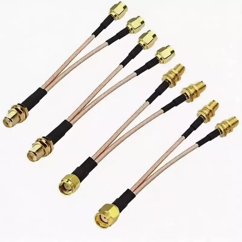
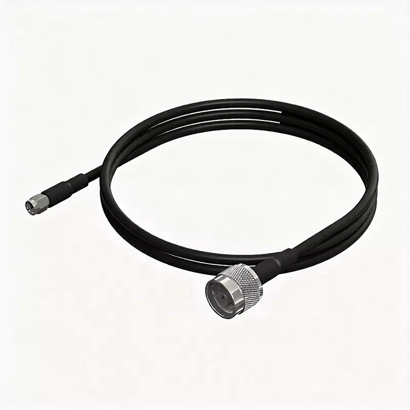
Technology Blog

pcb board

Differences Between Multilayer and Double-Layer PCB Board

As electronic products demand increasingly diverse functionalities, pcb board structures have grown ever more complex. Constrained by spatial limitations, PCB circuit boards have progressively “evolved” from single-layer to double-layer and ultimately multi-layer designs. What, then, distinguishes the manufacturing processes of multi-layer PCB boards from those of double-layer PCBs? A multilayer pcb board is a type […]

ionic cleanliness

Ionic cleanliness Testing Methods and Importance for PCB Boards

Ionic cleanliness testing serves as a critical quality control measure for evaluating ionic contaminant levels on pcb boards surfaces. Its primary objective is to prevent electrical faults such as short circuits and corrosion caused by ionic residues, thereby enhancing the reliability of electronic products. Employing techniques such as chemical extraction and conductivity measurement, this test

fr1 pcb

Characteristics and Applications of FR1 PCB

FR1 pcb is constructed from glass fiber-reinforced epoxy resin laminates. FR1 PCBs are rigid, flat materials composed of thin copper layers on a non-conductive phenolic resin substrate. FR1, fully known as Flame Retardant 1, is a PC film with high insulation and flame-retardant properties. This material not only exhibits excellent flame resistance but also possesses

PCB laser depaneling

Application and Advantages of PCB Laser Depaneling Technology

In electronic manufacturing, circuit boards must be divided into distinct sections to meet the design requirements of various electronic products. Traditional mechanical cutting and punching techniques struggle to satisfy modern production standards. The advent of PCB laser depaneling machines has made this process efficient and precise, not only boosting production efficiency but also ensuring the

osp

OSP process ensures stable PCB performance

OSP (Organic Solderability Preservative) is a surface treatment process for PCBs (Printed Circuit Boards). It involves coating the copper foil surface with an extremely thin organic protective film (approximately 0.2-0.5μm thick) to prevent copper oxidation and maintain solderability. During soldering, high temperatures cause the protective film to decompose, exposing the copper surface to bond with

fpc

The Role and Challenges of FPC in the 5G Era

What does FPC stand for? FPC stands for Flexible Printed Circuit, known in Chinese as a flexible printed circuit board, commonly abbreviated as a flexible board. FPC is a highly reliable, exceptionally flexible printed circuit board manufactured using polyimide or polyester film as the substrate material, also referred to as a flexible circuit board or

pcba

PCBA Component Spacing Design

Component spacing design on PCBA represents a pivotal aspect of electronic product development, where precision directly influences circuit electrical performance, thermal efficiency, manufacturing feasibility, and the stable operation of the final product. Component spacing is not merely a matter of spatial allocation, but rather an art form that comprehensively considers electrical safety, thermodynamics, signal integrity,

Exposed Copper PCB Trends and Quality in Electronics

Exposed Copper PCB Trends and Quality in Electronics

Definition and Basic Characteristics In the design and manufacturing of printed circuit boards (PCBs), exposed copper refers to surfaces with exposed copper, not covered by solder or solder mask. Exposed copper typically appears in areas requiring subsequent soldering, grounding, or testing, such as pads, vias, or conductive bridges. Compared to PCBs fully covered with solder

led light pcb design

Key Considerations in LED Light PCB Design

LED lighting products’ efficiency, energy-saving properties and extended lifespan have driven their increasing market prevalence. At the core of these products, LED light pcb design is pivotal in ensuring luminaire performance, thermal management and reliability. This article delves into each stage of the LED PCB design process to assist you in creating an outstanding LED

pcb board

Common PCB Board Defects and Countermeasures

In electronic manufacturing, PCB board quality forms the cornerstone for ensuring device performance and reliability. However, within complex production processes, multiple factors may induce various defects in PCBA, thereby compromising the final product’s functionality. This article delves into four prevalent defect categories in PCBA manufacturing: delamination, plated-through-hole copper fractures, pcb board warping and buckling, and

Future of Automated PCB Testing Machine in Smart Electronics Production

Future of Automated PCB Testing Machine in Smart Electronics Production

Introduction In modern electronics manufacturing, printed circuit boards (PCBs) are considered the “heart” and “nervous system” of electronic products. From smartphones and wearables to automotive electronics, medical devices, and aerospace, the functionality of nearly all electronic products relies on PCBs. However, as PCBs accelerate toward higher density, miniaturization, and multi-layered design, quality issues are becoming

PCB chamfering

PCB Chamfering Technology Enhances Circuit Board Performance

PCB chamfering, simply put, involves bevelling the edges of printed circuit boards. This process is typically carried out after the boards have been cut, using specialised chamfering machinery or hand tools to transform the board’s right-angled edges into bevelled surfaces at a specific angle. This treatment not only enhances the aesthetic appearance of the circuit

pcba

PCBA contaminants and cleaning

The definition of PCBA contaminants refers to any surface deposits, impurities, inclusions, or adsorbed substances that reduce the chemical, physical, or electrical performance of the PCBA to an unacceptable level. The main aspects include the following: Classification of PCBA Contaminants Typical PCBA cleaning processes Solvent Cleaning Semi-Aqueous Solutions Water-based cleaning PCB ion cleanliness testing methods

Core Value and Future Development of Etched FPC in Electronics Manufacturing

Core Value and Future Development of Etched FPC in Electronics Manufacturing

Introduction In modern electronics manufacturing, flexible printed circuits (FPCs) have become a key technology for connecting miniaturized, high-performance electronic systems. As electronic products continue to evolve toward thinner, smarter, and more multifunctional designs, traditional rigid circuit boards are increasingly unable to meet the demands of complex spatial layouts and dynamic environments. In contrast, FPCs, with

UPS PCB

Classification and Design of UPS PCB

UPS PCB, short for uninterruptible power supply printed circuit board, is the core control board of the UPS system. It is primarily responsible for providing emergency power to equipment when the main power supply is interrupted. UPS PCBClassification ⑴ Offline Square Wave Output UPS Power Supply: Its single-unit output power is approximately 400–2000 VA. When

Flex assembly manufacturing process and quality control

Flex assembly manufacturing process and quality control

Introduction – The Importance of Flex Assembly and Industry Background As electronic products continue to evolve towards thinner, more compact, and higher-performance designs, traditional rigid PCBs are no longer able to meet the demands of some specialized applications. Therefore, flexible assembly has become an indispensable component of modern electronics manufacturing. It not only provides flexibility

PCB exposed copper

Causes and Solutions for False PCB Exposed Copper

After the PCB circuitry is etched, a layer of ink (green ink, blue ink, black ink, etc.) needs to be applied. However, ink is liquid and has flowability. During the curing process after application, uneven ink distribution may occur, primarily around drill holes. In such cases, certain areas may appear under a magnifying glass to

PCB manufacturing

PCB Manufacturing Expenses and Optimization

In today’s highly integrated electronic product era, circuit boards serve as core components, and pcb manufacturing costs directly impact the market competitiveness of the final product. Accurately understanding the composition of PCB expenses, mastering their calculation methods, and effectively implementing cost optimisation strategies are key to manufacturers and design engineers maintaining a competitive edge in

Presensitized PCB boards

What is a presensitized PCB board?

What is a presensitized PCB board?A presensitized pcb board is a special type of printed circuit board with a photosensitive surface. It supports photolithography technology and can be adjusted using ultraviolet light. Despite common misconceptions, presensitized PCBs are similar to standard copper-clad PCBs, but essentially involve transferring graphics onto the board. Presensitized printed circuit boards

pcb board

PCB board testing methods and advantages

PCB board serves as the core components of electronic products, and their quality directly impacts the performance and reliability of the final product. With the rapid advancement of electronic technology, PCB design has become increasingly complex, with higher density and integration levels. This has led to higher demands on PCB inspection, rendering traditional inspection methods

Everything You Need to Know About Soldering Wire

Everything You Need to Know About Soldering Wire

Introduction and Definition of Soldering WireIn modern electronics manufacturing, metalworking, and various electrical assembly processes, soldering is a crucial process for connecting components and conductors. Among the many soldering materials, soldering wire is one of the most common and essential soldering consumables due to its ease of use, wide applicability, and consistent soldering results. It

EMI shielding

Board-level EMI shielding technology in PCB design

EMI radiation consists of electric and magnetic fields, which disrupt the normal operation of electronic devices. These electromagnetic waves propagate within electronic devices and interfere with electrical components, with their ratio referred to as wave impedance. To reduce EMI, we use metal cans (Faraday cages) to encapsulate electronic circuits on printed circuit boards (PCBs), which

Leiterplatte Erdung

Key Considerations for PCB Grounding Design

The pcb grounding plane on a PCB is typically a large metal area connected to the circuit ground. This metal area may only occupy a small portion of the board or, in multi-layer designs, it can span an entire layer. Depending on design requirements, it may even span multiple layers. Grounding, in simple terms, is

How to Tell if Your Aquarite Control Board is Bad

How to Tell if Your Aquarite Control Board is Bad

Introduction – Why Pay Attention to the Health of Your Aquarite Control Board In swimming pool water quality management, automated salt chlorination systems are widely adopted for their efficiency, environmental friendliness, and reduced chemical use. The Aquarite Control Board, the “brain” of the entire salt chlorination system, is responsible for monitoring water salinity, controlling the

Scroll to Top