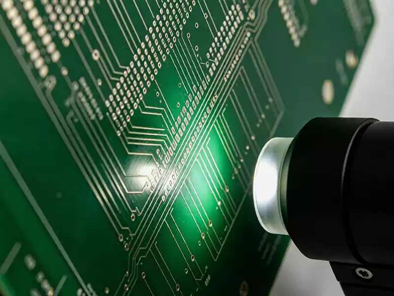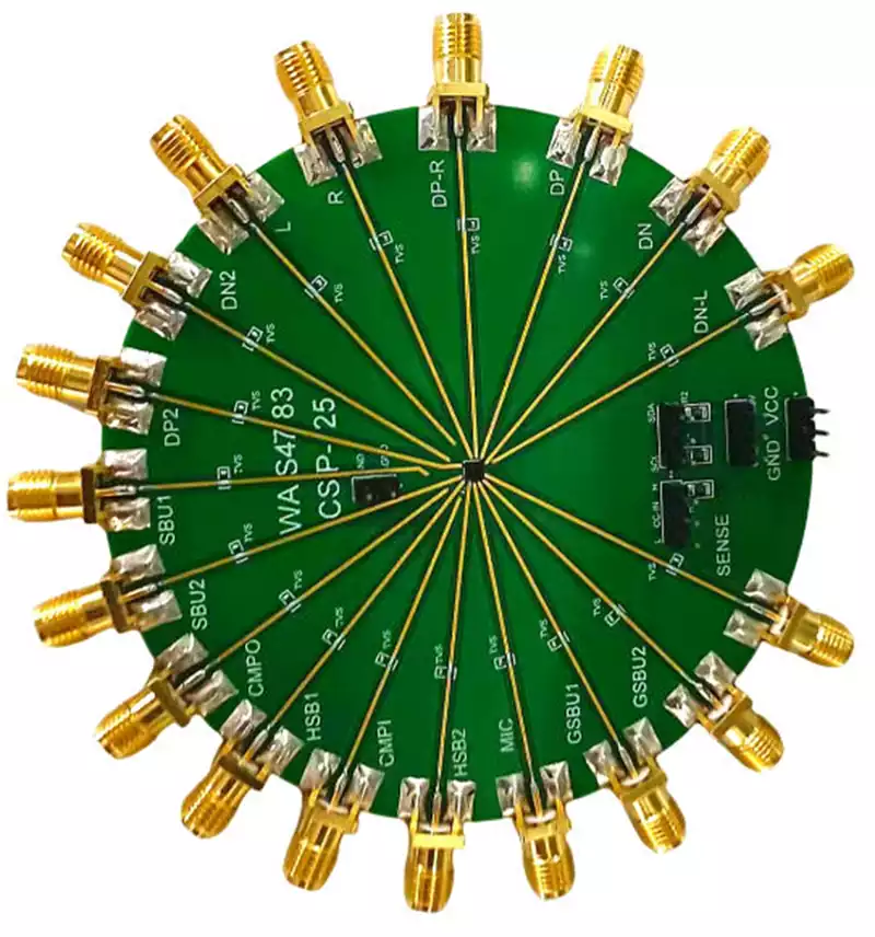
An In-Depth Analysis of Hardware PCB Proto Board Development
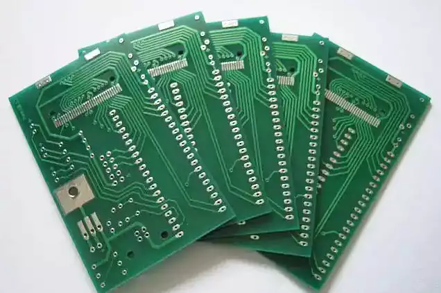
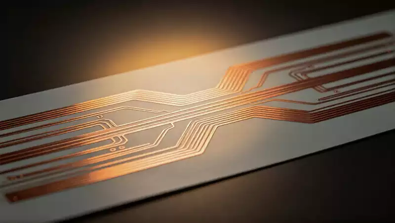
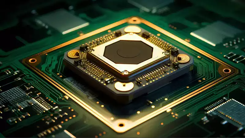
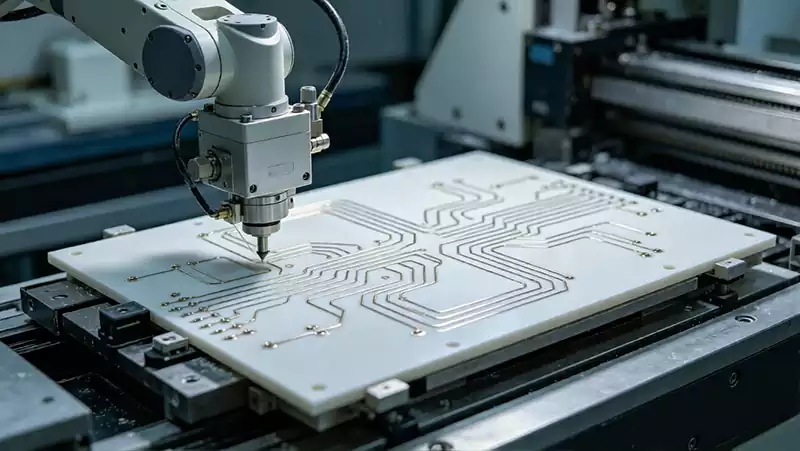
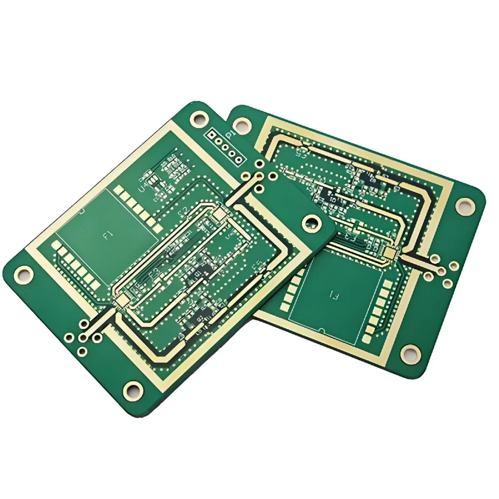
Redefining the PCB Proto board : A Core Hub and Risk Control Point in Hardware Product Development In the grand narrative of hardware innovation, the PCB prototype is often misunderstood as a simple, transitional “circuit verification object.” This perception is dangerous and costly. We must redefine it as a “miniature product” that undergoes the first […]