In the field of PCB design and assembly, through hole PCBs remain a core technology—even though surface-mount technology (SMT) now dominates most modern devices. Many engineers still opt for through hole PCBs when designing products that require high mechanical strength, high power handling capacity, or ease of maintenance.
In practice, you will find through hole PCBs in industrial control systems, automotive electronics and aerospace equipment. Their unique design — where component leads are inserted into drilled holes and soldered to the copper traces on the opposite side of the board — provides a more robust connection than surface-mount technology, making them ideal for components subjected to vibration or high-stress environments.
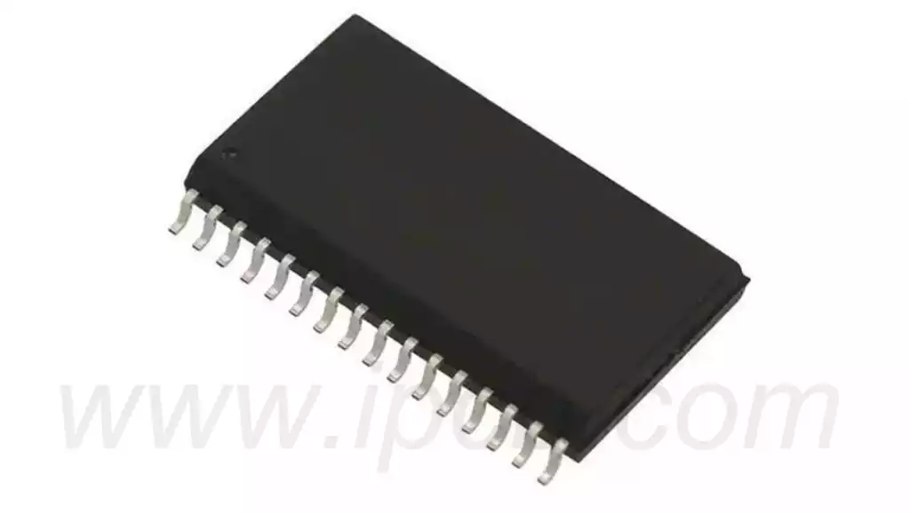
What is a through hole PCB?
A through hole PCB utilises drilled holes to mount components with leads. The component leads pass through these holes and are then soldered to the copper traces on the opposite side of the board. This design provides both mechanical retention and electrical connection.
Many designers confuse through-holes with vias, but the two are not the same concept. A via is a plated-through hole used to connect circuits on different layers of a PCB; component leads are not inserted into it. A through-hole, on the other hand, is specifically intended for component mounting — although in some cases, it can also serve to transmit signals between layers.
This distinction is crucial in layout design. Confusing the two often leads to errors in hole size or pad design, which in turn can cause assembly delays or board defects. I have seen many novice designers rush into the layout phase without carefully verifying the purpose of the holes, ultimately leading to such issues.
Fundamentals of Through-Hole Technology
Through-hole technology (THT) originated in the 1950s, decades before surface-mount technology. It remained the standard PCB assembly process until the late 1980s, when surface-mount components became popular due to their smaller size.
The assembly process is straightforward: components are inserted from the top of the board, with the leads passing through the drilled holes, and soldering is then completed either manually or using wave soldering equipment. Plated-through-holes (PTH) are the most common; the metal plating on the hole walls ensures the reliability of electrical connections between layers. Non-plated-through-holes (NPTH) are used solely for mechanical fixation and do not carry signal transmission functions.
In actual production, through-hole processing demands a high degree of drilling precision. The hole diameter must match the component lead dimensions, whilst allowing a clearance of 0.15–0.25 mm to facilitate lead insertion and ensure uniform copper plating on the hole walls — a detail that many novice designers tend to overlook. Such negligence can result in components becoming stuck during insertion or lead to poor solder joints later on.
Advantages of through hole PCBs:
Superior mechanical strength and connection reliability:
The leads of through-hole components pass through the entire PCB board and are soldered on both sides of the pads, creating a strong mechanical anchor.
This structure results in more robust solder joints that are far more capable of withstanding physical stresses (such as vibration, shock and insertion/removal forces) than surface-mount (SMT) solder joints.
They are particularly well-suited for applications requiring high-reliability connections, such as power connectors, high-power devices, external interfaces subject to physical insertion and removal (USB, power sockets, terminal blocks), automotive electronics, aerospace equipment, and certain industrial environments.
Superior thermal dissipation:
The component leads pass directly through the PCB board, providing an additional thermal conduction path.
The pins themselves can more effectively conduct heat generated by the components to the copper foil layers within the PCB board (inner layers) or to the heat dissipation areas on the reverse side.
For components that generate significant heat, such as power transistors, transformers and high-resistance components, through-hole mounting is the preferred or necessary choice, helping to prevent failure due to overheating.
Excellent current-carrying capacity:
Through-hole leads are typically larger and thicker than SMT pads.
The solder joints themselves are also larger, with a greater cross-sectional area.
This enables through-hole connections to carry higher currents (in amperes) than SMT joints of the same size, making them ideal for high-power applications and power supply circuits.
Convenience for prototyping, testing and repair:
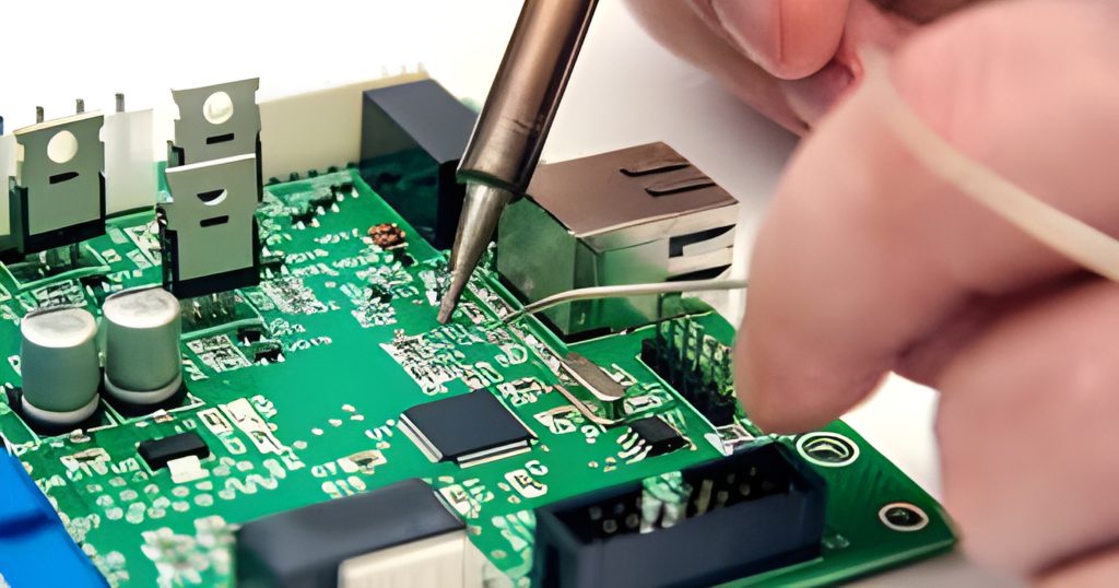
Easy manual soldering/rework: Through-hole components are well-suited to manual soldering, breadboard experiments and desoldering during repairs (easier to operate with a desoldering pump or soldering iron). This makes them highly suitable for prototyping, education, DIY and small-batch production.
Ease of Jumpering/Modification: Larger through-hole pads facilitate the use of jumper wires or the temporary addition of components during debugging or repairs.
Manual Assembly Feasibility: For small batches or situations where automated production is not required, through-hole components can be inserted and soldered manually.
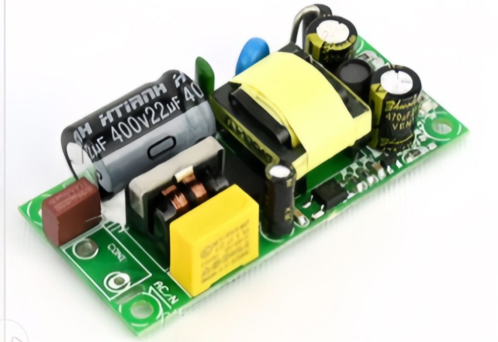
Stronger physical retention (for large/heavy components):
Bulky or heavy components (such as large electrolytic capacitors, inductors, connectors, and heat sink bases) may not be securely held in place by the adhesion of surface-mount solder joints alone.
The through-hole pins provide mechanical retention, which, combined with soldering, offers more reliable support for such components, preventing them from becoming dislodged or damaging solder joints under vibration, impact or gravity.
Greater component height flexibility:
Many classic or specialised components (such as certain types of connectors, switches, and high-voltage/high-power devices) may only be available in through-hole packaging. Opting for through-hole technology allows access to a wider range of components.
Key Design Specifications for Through hole PCBs (Including IPC Standards)
Good design can prevent most assembly issues. Adhering to IPC standards—particularly IPC 610A, J-STD-001 and IPC 7251—ensures that your Through hole PCBs are manufacturable and reliable.
Via size design is critical. The finished hole diameter should be the maximum diameter of the component lead plus a clearance of 0.15–0.25 mm, depending on layout density. High-density boards use a 0.15 mm clearance (Class C), whilst industrial-grade, high-reliability designs use a 0.25 mm clearance (Class A). This clearance prevents damage to the leads during insertion and ensures uniform plating on the hole walls.
Pad dimensions must not be overlooked. The width of the pad ring (the copper foil surrounding the hole) should be at least 0.2 mm for Class A designs, 0.15 mm for Class B, and 0.1 mm for Class C. If the pad ring is too small, the pad is prone to detachment during soldering or when subjected to mechanical stress.
Component spacing is also a critical factor. A minimum spacing of 1.5 mm must be maintained between through-hole components to prevent bridging during wave soldering. For components with thicker pins (such as power connectors), the spacing must be increased to 2 mm or more to prevent localised overheating during soldering.
Common Manufacturing Defects and Solutions
Poor solder joints are one of the most common issues. This is primarily caused by insufficient temperature or speed during wave soldering, resulting in the solder not melting completely and failing to bond properly with the pins and pads. The solution is simple: reheat the solder joint with a soldering iron to ensure the solder flows sufficiently.
Voids in the copper plating of through-hole (PTH) components are also a common issue. Tiny gaps in the plating on the hole walls can lead to poor electrical contact, usually caused by inadequate cleaning of the board prior to plating or uneven plating current. To resolve this, ensure the board is thoroughly cleaned before plating and adjust the plating parameters to guarantee uniform coverage.
Damage to component leads is also common, particularly with fine-lead components. This is usually caused by forcing components into holes that are too small. The solution is straightforward: verify the lead diameter against the hole diameter before drilling, and allow for appropriate clearance based on the design density.
Through-hole vs Surface Mount Technology (SMT): Which to Choose?
The choice between through-hole technology and surface mount technology depends on the specific requirements of the product application. In practice, many modern PCB boards utilise both technologies simultaneously to fully leverage their respective strengths.
Through-hole technology performs particularly well in scenarios requiring high reliability and high power handling capacity. If a circuit board needs to withstand vibration (such as in automotive electronics or industrial equipment), or must cope with high voltage and high current, through-hole technology is often the more suitable choice. Furthermore, through-hole components facilitate repair and are well-suited to prototyping, making them particularly suitable for small-batch projects.
Surface Mount Technology (SMT), on the other hand, is better suited to miniaturised, high-density PCB designs and is widely used in products such as smartphones, laptops and wearable devices. In high-volume production, SMT offers higher assembly efficiency; its smaller component size also helps to save board space. However, relatively speaking, SMT lacks the mechanical stability of through-hole technology and is more difficult to repair.
Cost is also a factor that cannot be overlooked. Through-hole technology requires an additional drilling process and has a slower assembly speed, resulting in higher costs during mass production; whilst surface-mount technology, although requiring a significant initial investment in equipment, offers a lower unit cost during mass production.
Applications of through hole PCBs
Industrial Control and Automation
In scenarios such as automated factory production lines, industrial robots and power control systems, through hole PCBs, with their excellent mechanical stability, can withstand harsh industrial environments characterised by high temperatures, high humidity, strong electromagnetic interference and frequent mechanical vibrations. For example, PLC (Programmable Logic Controller) control boards mostly utilise Through hole PCBs to ensure the accurate transmission of control commands during prolonged continuous operation, thereby guaranteeing the stable functioning of production lines.
Education and Research
In school electronics laboratory courses and during the prototype development phase at research institutions, through hole PCBs are the preferred choice for teachers, students and researchers due to their ease of manual soldering and debugging. Students can build simple circuits on through hole PCBs to gain an intuitive understanding of electronic circuitry and verify theoretical concepts; researchers developing prototypes for new electronic products can also utilise through hole PCBs to rapidly implement circuit functions, flexibly adjust design schemes and accelerate the research process.
Certain Modules in Consumer Electronics
Although consumer electronics are generally moving towards miniaturisation, through hole PCBs still hold a place in internal modules where space requirements are not stringent and cost is a key consideration, such as in certain audio equipment and the mainboards of traditional televisions. They can reduce production costs whilst meeting basic functional requirements, thereby enhancing the product’s value for money and enabling consumers to acquire their desired products at more affordable prices.
Through hole PCBs remain indispensable in high-reliability and high-power applications; when used in conjunction with SMT, they achieve the optimal balance between performance and cost.