In the vast field of modern wireless communication and cutting-edge electronic engineering, radio frequency (RF) technology undoubtedly forms the invisible backbone supporting this interconnected world. From the 5G millimeter-wave antennas in our smartphones to the 77Hz collision avoidance radars in self-driving cars that constantly sense their surroundings, and the low-orbit satellite communication links soaring in deep space, high-frequency electromagnetic waves are traversing the boundary between physics and digitality at the speed of light. And in these extremely sophisticated electronic systems, the fundamental physical carrier that carries and transmits these high-frequency microwave signals is the RF printed circuit board (PCB).
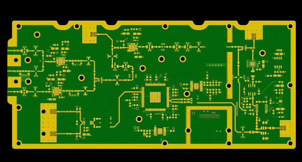
In low-frequency or purely digital circuit design, PCBs are often simply regarded as a “collection of wires” and a “mechanical support platform” for connecting various electronic components. However, when the operating frequency of signals enters the RF, microwave, or even millimeter-wave bands, the electromagnetic laws of the physical world undergo a fundamental change. At this point, the PCB is no longer a simple connector; every copper trace, every tiny via, and even the microscopic molecular structure of the insulating substrate itself constitutes a complex network of distributed parameters. The RF PCB Materials selection is no longer merely an insulator but becomes part of the electromagnetic wave transmission medium. Therefore, in the field of radio frequency (RF) engineering, the choice of materials directly determines the success or failure of the entire system. This is a top-level competition involving electromagnetics, materials polymer chemistry, thermodynamics, and precision manufacturing processes.
Deconstructing the Physical Environment and Core Electromagnetic Parameters of RF Signals
To deeply understand the selection logic of RF circuit board materials, we must first discuss the physical nature of high-frequency electromagnetic wave propagation in solid media. The most widely used epoxy resin fiberglass cloth substrate in traditional consumer electronics products reveals fatal flaws when facing RF signals. This is because high-frequency alternating electric fields cause severe polarization of the polar molecules within the material, resulting in huge energy consumption and severe signal distortion. In the RF field, the two most crucial electromagnetic physics indicators for evaluating the quality of a material are the dielectric constant and the dielectric loss tangent.
The dielectric constant, in physics, is a physical quantity that characterizes the degree of polarization of a dielectric under the influence of an electric field. In RF circuit board design, you can visualize it as a “deceleration coefficient” and a “capacitive reservoir” for electromagnetic waves propagating within the material. The higher the dielectric constant, the slower the electromagnetic waves propagate in the medium, and the greater the parasitic capacitance generated by the trace to the reference ground plane. In microwave antenna design and microstrip line impedance matching, the dielectric constant directly determines the physical width of the signal line and the geometry of the antenna resonant element. If the dielectric constant of the material fluctuates or varies between different batches, it will cause a shift in the carefully designed 50-ohm characteristic impedance, leading to strong reflections of the RF signal in the transmission channel, forming severe standing wave phenomena, ultimately resulting in ineffective transmission of transmit power and a significant decrease in receiver sensitivity.
The dielectric loss tangent is figuratively referred to by engineers as the “hidden tax” on RF energy. When ultra-high frequency alternating RF signals pass through an insulating medium, the polymer chains and polar groups inside the substrate undergo intense micro-friction due to the high-speed reversal of the high-frequency electric field. This molecular-level friction directly converts valuable RF electromagnetic energy into useless heat energy, which is dissipated. The higher the operating frequency, the more intense this friction, and the energy loss increases exponentially. At frequencies of a few gigahertz, the loss of ordinary substrates can completely absorb weak RF received signals. Therefore, finding materials with extremely low dielectric loss is a perpetual pursuit in RF circuit board materials science.
The stringent challenges of environmental stress and thermodynamics
In practical engineering applications, RF devices are often deployed in extremely harsh physical environments. Whether it’s an outdoor 5G macro base station exposed to the scorching sun or an airborne radar flying at extremely cold altitudes, drastic temperature fluctuations pose stringent challenges to RF circuit board materials that go beyond the realm of pure electromagnetics. At this point, thermodynamic parameters become another core pillar in material selection.
The most prominent is the thermal temperature coefficient of the dielectric constant. Common sense in the physical world tells us that the properties of most materials change with temperature, and the dielectric constant is no exception. If the thermal temperature coefficient of the dielectric constant of an RF board is too large, it means that when the device operates from the freezing point of winter to the high temperature of summer under full load, the dielectric constant of its substrate will drift significantly. This drift is catastrophic for systems that rely on extremely precise phase control (such as the antenna array of phased array radar or multi-channel base station transceiver systems). A drift in the dielectric constant can cause unpredictable phase differences between channels, resulting in severe divergence and deflection of the originally focused radar beam. Therefore, top-tier RF materials must possess extremely low temperature coefficients of dielectric constant to ensure absolute stability of electromagnetic properties over a very wide temperature range.
Secondly, there’s the material’s coefficient of thermal expansion. Printed circuit boards (PCBs) are composite materials made of copper foil, resin systems, and glass fibers. The coefficient of thermal expansion of copper as a metal naturally differs significantly from that of the polymer in organic resins. In modern high-density interconnected multilayer RF PCBs, engineers must connect RF signals across different layers using densely packed metallized vias. When the PCB is subjected to the high temperatures (over 250 degrees Celsius) of lead-free reflow soldering for surface mounting, or to repeated thermal shock cycles in actual use, the substrate expands dramatically in the direction perpendicular to the board surface (i.e., the thickness direction). If the material’s coefficient of thermal expansion is too high, this enormous mechanical expansion stress can forcefully break the fragile electroplated copper layer inside the via walls, causing complete system failure. To address this issue, radio frequency (RF) materials often require the addition of large amounts of special inorganic ceramic fillers. The extremely low thermal expansion of ceramics helps to restrain excessive resin expansion, thus ensuring the absolute reliability of the three-dimensional interconnects within the multilayer board.
Furthermore, water absorption rate is a critical factor for RF materials. Pure water has a dielectric constant of around 80 at room temperature, while excellent RF materials typically have a dielectric constant of around 3. This means that even if the substrate absorbs only a tiny amount of moisture from humid air, the extremely high polarity of water molecules will instantly increase the overall dielectric constant of the composite material, causing a significant deterioration in dielectric loss. Therefore, the polymer framework of RF materials must possess extremely excellent hydrophobicity to chemically prevent water molecule penetration.
The Pinnacle Showdown of Mainstream RF Polymer Material Systems
Looking at the global leading RF substrate market, the evolution of material systems is essentially a technological history of blending polymer chemistry and inorganic nanopowder physics. Currently, the core RF materials in the industry are mainly divided into three schools of thought, each seeking the ultimate balance between performance and processing difficulty.
At the very top of the loss performance pyramid is the polytetrafluoroethylene (PTFE) resin system. PTFE, also known as Teflon, has a molecular structure composed of tightly bonded carbon and fluorine atoms. Fluorine atoms are extremely electronegative elements in nature, tightly encasing the carbon chains to form an extremely stable and symmetrical nonpolar molecular configuration. This perfect nonpolar structure allows PTFE to experience almost no molecular friction in extremely high-frequency alternating electric fields, thus endowing the material with near-perfect ultra-low dielectric loss and extremely low water absorption. In fields with extremely stringent loss requirements, such as millimeter-wave radar and high-frequency satellite communications, it is undoubtedly the king. However, PTFE also has significant drawbacks: it is too soft and has an extremely smooth surface, exhibiting strong chemical inertness. Ordinary copper foil simply cannot adhere to its surface. To manufacture it into circuit boards, factories must use extremely expensive surface activation processes such as plasma bombardment to roughen the material surface. Simultaneously, its soft texture poses a significant risk of physical deformation during drilling and multilayer lamination processes.
To address the engineering challenges of processing pure polytetrafluoroethylene (PTFE), hydrocarbon resin systems have emerged. These are thermosetting materials with a molecular structure similar to traditional epoxy resins, but with deeply optimized high-frequency electrical properties. The greatest innovation of hydrocarbon resin systems lies in their unique cross-linking reaction, which allows them to retain the excellent high-frequency, low-loss characteristics of PTFE while achieving almost identical mechanical rigidity and processing yield to traditional epoxy resins. They can be easily laminated, drilled, and metallized into multilayer boards like ordinary circuit boards, without requiring stringent plasma treatments. For mass-produced 5G macro base station antenna elements and microwave RF front-end modules, hydrocarbon resin composites have found the perfect balance between RF performance, manufacturability, and cost.
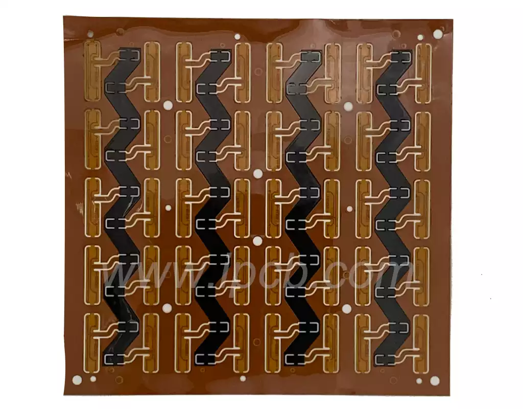
Furthermore, with the rise of wearable devices, flexible smart terminals, and high-frequency liquid crystal antennas, liquid crystal polymers and polyimide, two flexible RF materials, are beginning to shine. Especially within the extremely confined space of smartphones, liquid crystal polymers have become the ultimate material for flexible RF transmission lines due to their superior high-frequency, low-loss characteristics even at extremely thin thicknesses, as well as excellent moisture-proof and water-resistant properties, enabling high-density integration of millimeter-wave antenna arrays and RF chips.
The Deep Entanglement of Microscopic Roughness and High-Frequency Skin Effect
In RF circuit board design, focusing solely on the insulating substrate is destined to fail. This is because in this high-frequency world, the main body of electrical energy flow—the copper foil—is also undergoing awe-inspiring physical transformations.
In low-frequency direct current, the current flows uniformly across the entire cross-section of the copper conductor. However, as the frequency climbs to the gigahertz level, the remarkable electromagnetic “skin effect” begins to dominate. Due to the mutual cancellation of eddy currents generated by the high-frequency alternating magnetic field inside the conductor, the current of the high-frequency signal is pushed towards the surface of the copper foil by an extremely strong electromagnetic force, flowing close to a very thin layer of space. When the frequency reaches 77 gigahertz, the “skin depth” of the actual current flow is less than one micrometer. At this point, the microscopic morphology of the copper foil surface becomes crucial in determining the survival of the signal. In traditional circuit board manufacturing, to ensure the smooth copper foil adheres firmly to the resin substrate, it undergoes an electrochemical roughening treatment before leaving the factory, creating countless tiny “copper teeth” on its surface, resembling miniature peaks. These micrometer-sized copper teeth, like tree roots, penetrate deeply into the resin, providing strong mechanical peel strength.
However, under the influence of the skin effect, the radio frequency current is forced to trudge along the contours of these microscopic peaks. This significantly lengthens the actual current transmission path. Physics dictates that the longer the path, the greater the conductor’s resistance loss. Furthermore, these sharp copper teeth generate localized electromagnetic field concentration effects in the microwave band, further exacerbating energy radiation and attenuation.
Therefore, in high-end radio frequency circuit boards, engineers must completely abandon traditional rough electrolytic copper foil and instead use ultra-low profile or even extremely low profile copper foil pressed using special processes. These special copper foils exhibit an extremely smooth, mirror-like finish under a microscope, with their microscopic surface roughness strictly controlled at the nanometer level, thus paving a smooth “highway” for high-frequency skin current. However, this brings a new process paradox: the extremely smooth copper foil is very difficult to bond firmly with resin. Therefore, materials scientists had to develop more advanced chemical bonding agent technology, no longer relying on physical “copper tooth anchoring,” but utilizing the power of chemical molecular bonds to tightly lock the mirror-like copper foil to the RF substrate, perfectly balancing ultra-low conductor loss and high reliable mechanical peel strength.
The final decision on hybrid multilayer architecture and surface treatment processes
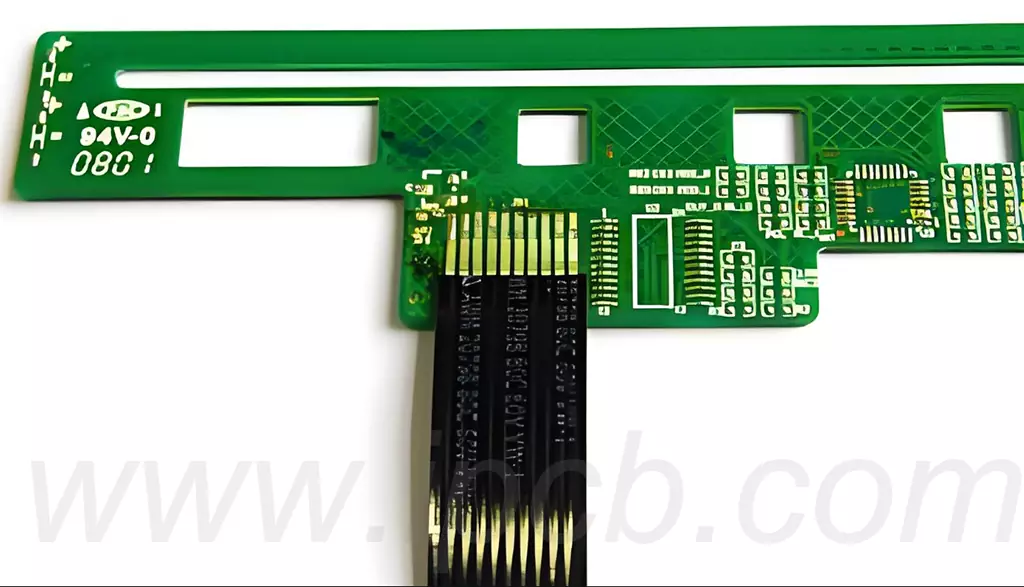
Once we have completed the selection of the substrate and copper foil, the RF circuit board enters the extremely complex multilayer physical stacking and manufacturing process. Modern electronic devices, due to extreme space constraints, generally cannot tolerate fabricating RF circuits and low-frequency digital control circuits on two different boards. Therefore, a hybrid multilayer lamination architecture has become the industry standard solution.
In this architecture, engineers place extremely expensive high-frequency RF materials on the outermost layer of the circuit board, specifically for carrying microstrip lines, antenna networks, and core RF components. Meanwhile, the inner layers use inexpensive, high-strength ordinary epoxy resin materials for low-frequency digital control signals and power lines. This hybrid material stacking design satisfies stringent RF performance requirements while keeping the overall manufacturing cost of the board highly competitive. However, bonding two materials with completely different physical properties together under high temperature and pressure requires overcoming the risks of board warping and delamination caused by mismatched coefficients of thermal expansion, as well as microscopic delamination due to poor adhesion between different resin systems. This severely tests the lamination process database and engineering expertise of printed circuit board manufacturers.
In the final step of manufacturing, the choice of surface treatment process directly determines the final radiation quality of the RF signal. Traditional circuit boards typically use chemical nickel plating (CCP) for oxidation prevention and easy soldering. This process deposits a layer of nickel on the copper pads, then coats the nickel with a thin layer of gold. In the low-frequency domain, this is an excellent anti-corrosion coating. However, in the RF microwave domain, the presence of nickel is a deadly poison. Because nickel is a typical ferromagnetic material, it generates enormous hysteresis and eddy current losses in high-frequency electromagnetic fields, instantly consuming the energy of radio frequency (RF) signals.
Therefore, genuine RF circuit boards resolutely avoid processes containing nickel during surface treatment. Engineers typically choose immersion silver plating because silver is the metal with the highest conductivity at room temperature. An extremely thin silver layer not only prevents oxidation of the copper substrate but also provides a lower resistance path for skin current. Alternatively, they may use a bare copper coating with an anti-oxidation film, directly retaining pure oxygen-free copper for the RF signal, using only a very thin organic chemical film to provide temporary anti-oxidation protection until the final component soldering. Every trade-off in process details paves the way for perfect RF signal transmission.
Conclusion: A Magnificent Symphony of Microscopic Physics and Macroscopic Engineering
After a thorough analysis of everything from dielectric constants, thermodynamic stability, and the evolution of polymer systems to the physical mechanisms of copper foil roughness under the skin effect, and then to the intricate engineering of multilayer hybrid architectures and surface treatments, it becomes clear that selecting materials for radio frequency printed circuit boards is far more complex than simply flipping through a few pages of datasheets or comparing a few parameters.
This is a systematic engineering art built upon electromagnetic field theory, spanning materials science, chemistry, and precision mechanical manufacturing. In this high-frequency microscopic world invisible to the naked eye, the polarization of any molecular chain, the undulation of any one-micrometer copper tooth, or the minute stretch caused by thermal expansion, will be amplified in the macroscopic system into severe signal distortion, reduced communication distance, or even blind spots in the entire radar system.
As human communication technology advances towards the terahertz band and future sixth-generation mobile communication technologies, the wavelengths of electromagnetic waves will become increasingly shorter, and the physical sensitivity of radio frequency (RF) signals to the transmission medium will reach unprecedented levels. The search for lower-loss resin frameworks, smoother and stronger-adhesion metal conductors, and the development of more highly integrated three-dimensional RF packaging substrate materials will continue to lead the forefront of global electronic materials science. Every small technological breakthrough in the field of RF substrates will transform into invisible electromagnetic wings, propelling humanity further and more clearly in its vast journey of exploring the information universe.