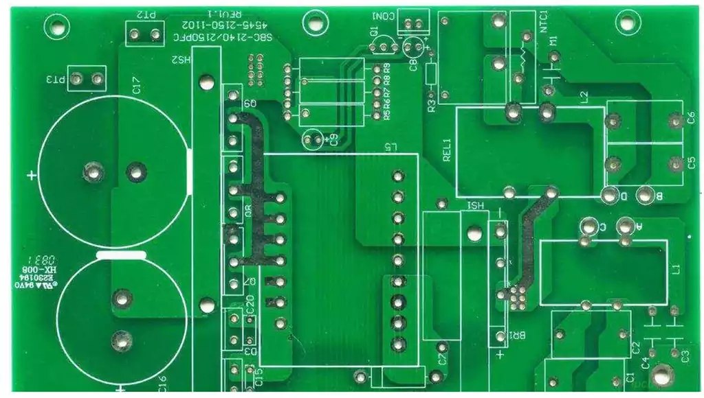
HDI PCB, or High Precision, High Density Interconnect Printed Circuit Board, is a type of circuit board characterized by high line width and line spacing, high wiring density, and tiny apertures. Compared to traditional PCB, it is able to achieve more complex circuit layouts in a smaller space, thus meeting the demand for miniaturization and high performance in modern electronic products. When designing it, engineers face many challenges, such as the processing difficulty of tiny line width and line spacing, the heat dissipation problem of high-density wiring, and the precision control of tiny apertures.
Key points of HDI pcb design
- Reasonable planning layout: In the design of HDI boards, it is necessary to reasonably plan the layout of each functional area to ensure that the signal transmission path is the shortest, reducing signal interference and loss.
- Optimize signal integrity: By reasonably selecting parameters such as line width, spacing and interlayer distance, the crosstalk and reflection of signals can be reduced and signal integrity can be improved.
- Introduce impedance control: When designing HDI board lines, the problem of impedance matching should be considered to improve the quality and stability of signal transmission.
When designing HDI pcb, the following principles and considerations need to be followed:
- Determine the function and performance requirements of the circuit: Before designing the HDI multilayer circuit board, you need to clarify the function and performance requirements of the circuit in order to provide guidance for the subsequent design.
- Select the appropriate materials and processes: According to the requirements of the circuit, select the appropriate base material, pre-coating materials (such as photographic ink) and solder resist materials, etc..At the same time, it is also necessary to select the appropriate process parameters to ensure the quality of the circuit board.
- Optimize the wiring layout: When designing HDI pcb, it is necessary to optimize the wiring layout to improve the performance and reliability of the circuit. This includes the reasonable allocation of the signal layer, ground plane layer and power layer location, as well as optimize the direction of the signal lines.
- Control impedance: impedance control is an important part of HDI pcb design. Through reasonable layout and selection of appropriate materials, impedance can be effectively controlled to improve the performance of the circuit.
- Consider thermal issues: In the design of HDI multilayer circuit boards, thermal issues need to be considered. Thermal problems can be effectively solved through a reasonable layout and selection of appropriate heat dissipation methods.
- Pay attention to dimensional accuracy: Since HDI multilayer circuit boards are manufactured using microvia technology, their dimensional accuracy requires high precision. In the design process, attention needs to be paid to the control of dimensional accuracy.
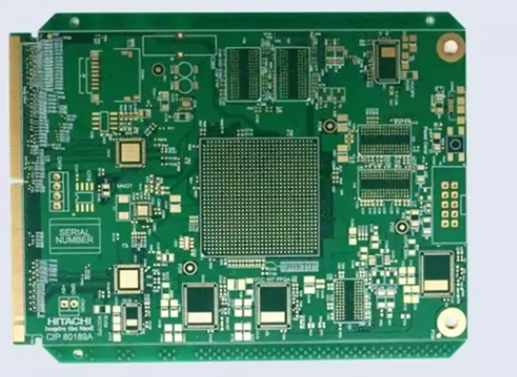
Compliance with relevant standards and specifications: When designing HDI multilayer circuit boards, it is necessary to comply with relevant standards and specifications to ensure the quality and reliability of the board.
HDI PCB design, as one of the core technologies of modern electronics manufacturing, is driving the continuous innovation and progress of electronic products with its advantages of miniaturization and high-density interconnection. With the continuous progress of technology and the continuous expansion of application areas, it will play a more important role in the future to create a better life for mankind.
