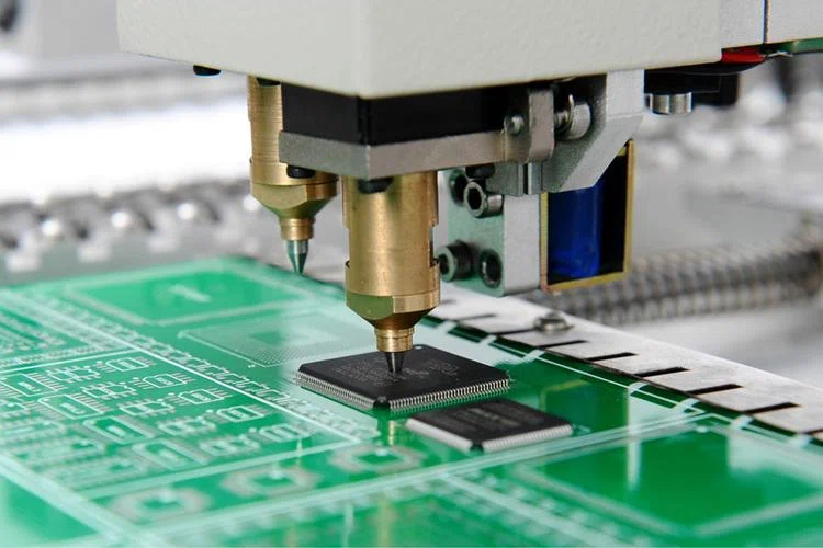
The success or failure of signal transmission in high frequency PCBs is often determined by details imperceptible to the naked eye. Via holes, serving as the core conduits for interconnecting signals between PCB layers, may appear merely as minute apertures piercing through the board layers. Yet in high frequency scenarios, they become the ‘invisible killers’ responsible for signal energy loss. Frequently, seemingly flawless high frequency PCB designs suffer from signal attenuation, impedance mismatch, and heightened crosstalk due to suboptimal via design. This results in unnecessary signal energy dissipation, ultimately compromising the performance and stability of the entire product.
The transmission characteristics of high frequency signals (typically above 1GHz) differ markedly from low-frequency signals. Issues such as the skin effect, parasitic parameters, and signal reflection are dramatically amplified, with the structural design of vias directly determining the severity of these problems. For the PCB manufacturing industry, mastering via optimisation techniques not only effectively reduces signal energy loss in high frequency PCBs and enhances product competitiveness but also serves as a key indicator of a company’s technical prowess. Resolving signal loss issues caused by vias requires no complex equipment upgrades. Precise control over core via design principles alone enables efficient signal energy transmission.
The Core Cause of high frequency PCB Signal Energy Loss Due to Via Holes
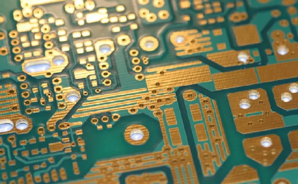
Parasitic parameters constitute the fundamental issue causing signal loss through via holes. The structure of vias—including their walls, pads, and solder mask layers—induces parasitic capacitance and inductance: parasitic capacitance causes phase shift in high frequency signals, reducing transmission speed while leaking signal energy; parasitic inductance increases signal impedance, leading to impedance mismatch and signal reflection. Even non-reflected signal energy suffers attenuation due to inductive loss. For ultra high frequency PCBs operating above 10GHz, losses induced by parasitic parameters may even surpass those inherent to the transmission line itself, becoming the primary cause of signal energy depletion.
Signal reflection and radiation losses constitute another significant source of dissipation stemming from suboptimal via design. When parameters such as via aperture, pad dimensions, and wall thickness fail to align with the transmission line, reflections occur at the via. These reflected signals superimpose with the incident signal, not only squandering energy but potentially inducing standing waves that further exacerbate energy loss. Simultaneously, vias act as ‘electromagnetic radiation sources’ on the PCB. When high frequency signals pass through, electromagnetic radiation is generated, causing partial signal energy to leak as electromagnetic waves. This reduces transmission efficiency and may interfere with surrounding signals.
Furthermore, manufacturing defects in vias exacerbate signal energy loss. For instance, uneven plating on the hole walls, pinholes, or voids increase the contact resistance of the via, leading to higher conductor losses. excessively thick or uneven solder mask coverage introduces additional dielectric losses, further depleting signal energy; and poor transition between the via and transmission line creates an ‘impedance discontinuity point,’ inducing signal reflection and causing energy dissipation. These seemingly minor details exert a critical impact on signal transmission in high frequency scenarios.
Four Key Approaches to Reducing Signal Energy Loss in Via Holes
First Optimisation Dimension: Precise Control of Via Dimensions to Reduce Parasitic Parameters. The aperture and pad size of via holes directly determine the magnitude of parasitic capacitance and inductance. Smaller dimensions yield lower parasitic parameters and consequently less signal energy loss. In high frequency PCB design, prioritising micro-vias (aperture 0.2–0.4mm) over traditional large-aperture vias (aperture 0.6mm+) effectively reduces parasitic capacitance and inductance, thereby minimising signal energy loss.
Concurrently, via pad dimensions must be appropriately matched. Pad diameters should not be excessively large, typically maintained at 2–2.5 times the via aperture diameter. This prevents increased parasitic capacitance from oversized pads while ensuring soldering reliability.
It is important to note that smaller via dimensions are not universally preferable; decisions must be made holistically considering PCB thickness, laminate structure, and manufacturing processes. For instance, in high frequency PCBs with substantial thickness, excessively small via diameters may complicate plating of the via walls, leading to defects such as uneven plating or pinholes, which can exacerbate signal loss. Therefore, via sizing must balance ‘parasitic parameter control’ with ‘manufacturing feasibility’, avoiding excessive miniaturisation that increases manufacturing complexity and cost.
The second optimisation dimension: Refining via structure to minimise signal reflection. The primary cause of signal reflection is impedance mismatch between vias and transmission lines. Consequently, the key to optimising via structure lies in achieving impedance matching and reducing impedance transitions. Two common optimisation approaches exist:
Firstly, employing ‘no-pad vias’ or ‘buried/blind vias’ designs. which minimises parasitic parameters and impedance transitions introduced by pads; blind/buried vias prevent through-hole penetration across the entire PCB, reducing signal radiation and reflection, particularly suited for multilayer high frequency PCBs. The second approach involves refining the transition structure between vias and transmission lines through tapered transition designs, avoiding direct perpendicular connections between transmission lines and vias to reduce impedance transition points and mitigate signal reflection.
For high frequency signal transmission, the advantages of buried blind vias are particularly pronounced. Traditional through-holes penetrating the entire PCB create longer hole walls, increasing parasitic inductance and radiation loss. In contrast, buried blind vias connect only adjacent layers, resulting in shorter hole lengths, lower parasitic parameters, and no exposure on the PCB surface, effectively reducing signal radiation. In ultra-high frequency PCBs for applications such as 5G millimetre-wave and automotive radar, buried blind via design has become a core technique for reducing via signal loss.
The third optimisation dimension: Rational via placement to control radiation loss and crosstalk. The layout of vias directly impacts signal radiation loss and crosstalk levels; improper placement exacerbates signal energy leakage while inducing mutual interference between adjacent signals. In high frequency PCB design, via placement must adhere to two core principles:
Firstly, avoid dense via placement, particularly for high frequency signal vias. Dense arrangements cause electromagnetic radiation to accumulate, increasing energy loss while exacerbating crosstalk. Secondly, position high frequency signal vias adjacent to ground vias. Ground vias form an ‘electromagnetic shielding enclosure’ that absorbs radiated energy from the vias, reducing signal leakage while lowering impedance and optimising signal transmission.
Furthermore, high frequency signal vias should be positioned as close as possible to transmission lines, minimising the distance between the line and the via to prevent energy dissipation from excessive transmission paths. Vias operating at different frequency bands should be separated to prevent high frequency vias from interfering with low-frequency ones, while also reducing their own radiated losses.
The fourth optimisation dimension: enhancing via manufacturing precision to reduce process losses. Manufacturing accuracy directly impacts a via’s electrical conductivity and structural integrity, with process defects significantly increasing signal energy dissipation. Therefore, optimising via manufacturing processes requires focusing on three key aspects:
Firstly, the via wall plating process. Employing a dual plating method of electroless copper plating followed by electrolytic copper plating ensures uniform wall plating thickness meeting specifications (typically 18-25μm), preventing defects such as pinholes, voids, or plating detachment, thereby reducing contact resistance.
Secondly, the solder mask process requires controlling uniform mask thickness to prevent coverage of the via pad, thereby minimising dielectric loss.
Thirdly, drilling precision must guarantee accurate via positioning and consistent aperture size, preventing connection failures between vias and transmission lines due to drilling deviations, which could cause impedance discontinuities and signal reflections.
Signal energy loss in high frequency PCBs appears multifactorial, yet vias—as the core interconnect between layers—directly determine transmission efficiency and stability through their design and manufacturing quality. Optimising vias presents no complex technical challenge. The core lies in addressing four key elements: parasitic parameters, impedance matching, radiation loss, and process precision. By tailoring via dimensions, structure, layout, and manufacturing processes to specific application scenarios and cost constraints, effective reduction of signal energy loss can be achieved.
With the rapid advancement of 5G and 6G communication technologies, high frequency PCBs are finding increasingly widespread application, demanding ever-higher signal transmission efficiency. Via optimisation will thus become an indispensable core technology within PCB design and manufacturing processes.
Looking ahead, as PCB manufacturing processes continue to advance and design techniques undergo sustained innovation, via optimisation methods will become more precise and efficient. This will further reduce signal energy loss in high frequency PCBs, providing robust support for the development of high frequency electronic equipment. Only by meticulously refining the details of via optimisation and exercising precise control over every design and manufacturing stage can we create more competitive high frequency PCB products, thereby securing a proactive position in industry competition.