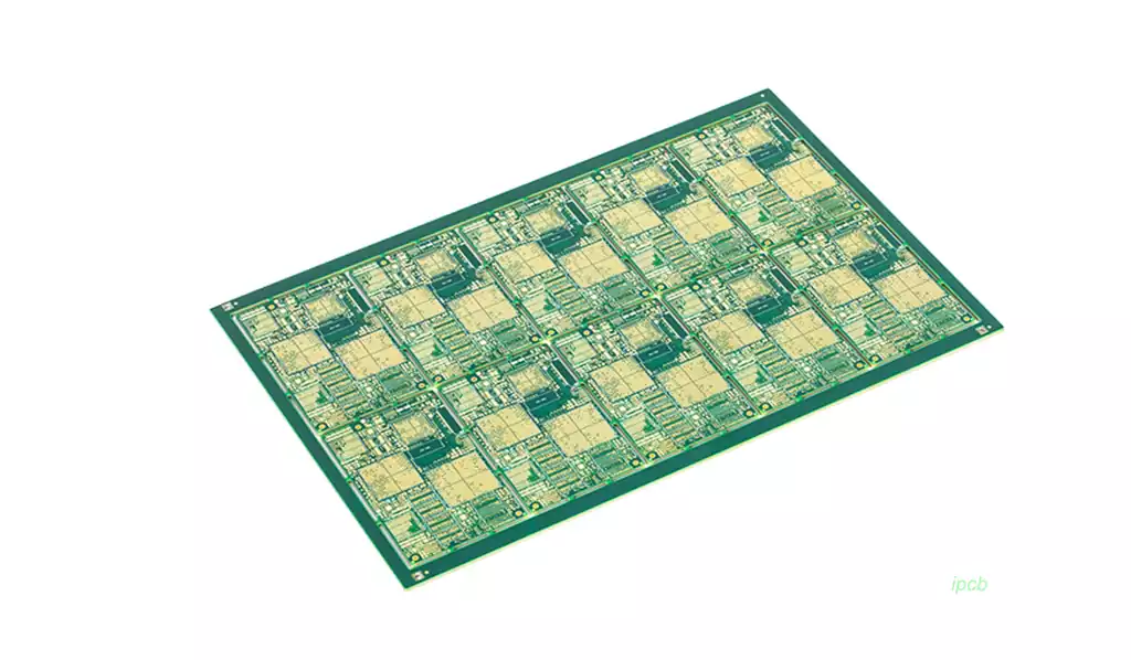
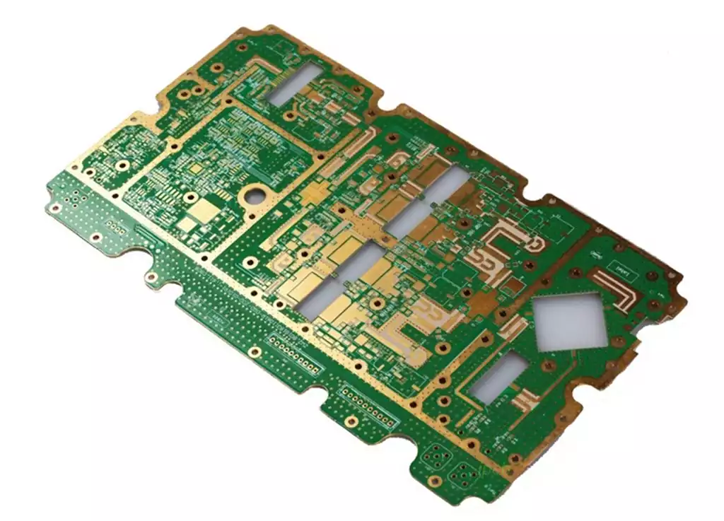
Compared to conventional printed circuit boards, high layer PCBs are characterised by greater board thickness, a higher number of layers, denser traces and vias, larger component dimensions, and thinner dielectric layers. This places higher demands on the utilisation of internal layer space, inter-layer alignment accuracy, impedance control and product reliability.
Key manufacturing challenges of high layer PCBs
1.Difficulty in controlling interlayer alignment
High layer count PCBs have a large number of layers, and customer requirements for interlayer alignment are becoming increasingly stringent, typically needing to be controlled within ±75 μm. However, factors such as large component dimensions, fluctuations in temperature and humidity within the pattern transfer workshop, cumulative misalignment caused by inconsistent thermal expansion and contraction of different core layers, and interlayer positioning methods make controlling interlayer alignment extremely challenging.
2.High difficulty in manufacturing inner-layer circuits
High layer pcbs often utilise special materials such as high Tg, high-speed, high-frequency, thick copper and thin dielectric materials, which impose stringent requirements on signal integrity (such as impedance control), thereby increasing the difficulty of manufacturing inner-layer circuits.
This manifests specifically as: narrow line widths and spacing, which are prone to open circuits, short circuits and micro-short circuits, resulting in low yield rates; dense circuits with multiple signal layers, increasing the risk of missed defects in inner-layer AOI; The inner core layers are thin, making them prone to wrinkling, poor exposure, and curling during etching; furthermore, as high layer PCBs are often system boards with large component dimensions, the cost of scrapping finished products is high.
3.Significant challenges in the lamination process
When laminating multiple inner core layers with prepreg, defects such as board slippage, delamination, resin voids and residual bubbles are likely to occur. The design of the laminate structure must fully consider material heat resistance, voltage resistance, resin content and dielectric thickness, and a reasonable lamination programme must be established. An increase in the number of layers makes it difficult to maintain consistency in expansion/contraction control and dimensional compensation factors; thin interlayer insulation layers can easily lead to failure in interlayer reliability testing (such as delamination following thermal stress testing).
4.Difficulties in Drilling
Specialised board materials—such as those with high Tg, high-speed, high-frequency, and thick copper—increase the difficulty of controlling drilling roughness, burrs, and removing drilling debris. A high number of layers leads to an accumulation of total copper thickness and board thickness, making drill bit breakage more likely; in dense BGA areas, narrow hole-to-hole spacing can easily cause CAF failures; and with thicker boards, skewed drilling is also a common issue.

Control of key production processes for high layer PCBs
1.Material Selection
With the increasing demand for high-frequency and high-speed signal transmission, high layer pcbs require copper-clad laminates with low dielectric constant (Dk), low dielectric loss (Df), low CTE, low water absorption and excellent performance. Common laminate suppliers (such as the A, B, C and D series) offer materials with varying characteristics.
For high-layer-count, thick-copper boards, pre-pregs with a high resin content should be selected to ensure sufficient resin flow to fill the inner layer patterns. Insulation layers that are too thick may result in excessively thick finished products, whilst those that are too thin may cause delamination or failure during high-voltage testing; therefore, material selection is of paramount importance.
2.Laminate Structure Design
During design, heat resistance, voltage withstand capability, resin flow, and insulation layer thickness must be comprehensively considered, adhering to the following principles:
The manufacturers of the prepreg and core board must be consistent.
Avoid using single sheets of 1080 or 106 prepreg (unless specifically requested by the customer); unless there are special requirements for dielectric thickness, the interlayer dielectric thickness should be ≥0.09 mm (IPC-A-600G).
For high Tg boards, both the core board and prepreg must be high Tg materials.
When the inner layer substrate is ≥3 oz, select prepregs with high resin content (e.g., 1080 R/C 65%, 106 R/C 73%, etc.), but avoid using only 106 high-resin prepregs to prevent glass fibre mat collapse, which can lead to dimensional instability or delamination.
The thickness tolerance of interlayer dielectric is generally controlled to ±10%; for impedance-controlled boards, this is managed to IPC-4101 C/M grade. If impedance is affected by substrate thickness, the board material tolerance must also meet C/M grade.
3.Control of Interlayer Alignment
It is necessary to accumulate production data to precisely compensate for the dimensional variations of each layer’s patterns, ensuring consistent expansion and contraction of the inner core layers. High-precision interlayer positioning methods (such as four-groove positioning Pin LAM or a combination of hot melt and rivets) should be adopted.
A reasonable lamination programme must be established, and routine maintenance of the press carried out, whilst controlling resin flow and cooling effects to minimise interlayer misalignment. Alignment control requires a comprehensive consideration of inner layer compensation values, positioning methods, process parameters and material properties.
4.Inner Layer Circuitry Process
Conventional exposure systems have a resolution of approximately 50 μm; the introduction of laser direct imaging (LDI) equipment can enhance this to around 20 μm. High-precision alignment exposure systems can improve pattern alignment accuracy to ±15 μm, whilst controlling interlayer alignment accuracy to within 30 μm, thereby significantly reducing alignment deviations in high layer PCBs.
Regarding circuit etching, in addition to conventional line width and pad compensation, fine compensation is required for special patterns such as looped traces and isolated traces. For traces with impedance or reactance requirements, it is necessary to verify whether the compensation is sufficient. Strictly control the composition of the etching solution; where necessary, upgrade to high-precision etching equipment to improve uniformity and reduce issues such as side etching, burrs and incomplete etching.
5.Laminating Process
Prior to lamination of high layer PCBs, positioning may be achieved using four-slot positioning (Pin LAM) or a combination of fusion bonding and riveting; OPE punching accuracy must be controlled within ±25 μm. The first board must undergo X-ray inspection for layer misalignment, and during mass production, the fusion bonding status of each board must be verified to prevent delamination.
Laminating programmes must be formulated based on the stack-up structure and material properties, appropriately reducing the heating rate and extending the high-temperature curing time to ensure sufficient resin flow and curing, thereby preventing board slippage and misalignment. Boards with different Tg values must not be laminated in the same oven; boards requiring standard parameters must not be mixed with those requiring special parameters; and process parameters for new, special materials must be validated in advance.
6.Drilling Process
Due to the thickness of the board and the copper layers, high layer count boards are prone to severe drill bit wear and breakage; therefore, the number of holes, feed rate and rotational speed should be reduced appropriately.
Accurately measure the board’s expansion and contraction to provide a compensation factor; for boards with 14 or more layers, hole diameters ≤ 0.2 mm, or distances between holes and traces ≤ 0.175 mm, a drilling machine with a positioning accuracy of ≤ 0.025 mm must be used. For holes with a diameter of 4.0 mm or greater, use step drilling; for aspect ratios of 12:1 or greater, use forward and reverse drilling. Where possible, use brand-new or single-grind drill bits, and control rough hole diameter to within 25 μm.
For high layer pcbs involving high-frequency, high-speed, and massive data transmission, back-drilling technology can effectively improve signal integrity; it is necessary to control the residual stub length, the alignment of drill holes between two passes, and the copper wires within the holes. Drilling machines with back-drilling capabilities should be selected, or equipment upgrades should be carried out; common back-drilling methods include traditional depth-controlled back-drilling, back-drilling of the inner signal feedback layer, and back-drilling to a depth proportional to the board thickness.
Reliability Testing
As system boards, high layer PCBs are thick, heavy and feature large component dimensions, resulting in high thermal capacity. Soldering requires greater heat input, necessitating a hold time of 50–90 seconds at 217°C (the melting point of tin-silver-copper solder), and cooling occurs at a slower rate. Consequently, the reflow soldering test duration must be extended accordingly. In accordance with IPC-6012C, IPC-TM-650 and industry standards, key reliability tests are conducted on high layer PCBs.
The manufacturing challenges of high layer PCBs span critical processes such as materials, patterning, lamination and drilling, imposing far stricter requirements on process consistency and control than those for conventional boards. Only through appropriate material selection, precise compensation and positioning, rigorous optimisation of process parameters, and targeted reliability verification can product yield and long-term stability be systematically ensured.