The rapid evolution of global computing networks and 5G/6G communication infrastructure is accelerating the transition of optical module data rates from 400G to 800G and even 1.6T. Within this high-speed transmission ecosystem, the optical module PCB serves as the fundamental platform for optoelectronic signal transmission, component integration, and thermal management. As a result, it has become a critical factor determining the stability, transmission performance, and service life of high-speed optical modules.
Unlike conventional PCBs, optical module PCBs designed for high-speed applications must meet extremely stringent requirements in signal integrity, routing precision, environmental reliability, and mass-production manufacturability. As optical modules continue to advance toward higher speeds, traditional PCB manufacturing limits are being challenged, giving rise to a series of technical bottlenecks while simultaneously driving comprehensive innovation in materials, processes, and design methodologies.
This article examines the major manufacturing challenges facing high-speed optical module PCBs, explores mainstream industry solutions, and analyzes future technology and market trends.
Four Core Challenges in High-Speed Optical Module PCB Manufacturing
As optical modules evolve toward higher bandwidths, four major technical barriers have emerged as unavoidable challenges for optical module PCB manufacturing.
1.Increasing Frequencies and Signal Loss Control
With per-channel transmission speeds advancing from 25 Gbps to 112 Gbps and beyond, high-frequency signal loss has become one of the most critical constraints affecting optical module PCB performance.
Signal attenuation increases with the square root of operating frequency. The 112G PAM4 signaling scheme contains abundant high-frequency harmonics, significantly increasing both conductor loss and dielectric loss. Conventional FR4 materials, with a dielectric constant (Dk) of approximately 4.4 and a dissipation factor (Df) ranging from 0.01 to 0.015, are suitable for low-speed applications but exhibit severe signal degradation in high-speed optical modules. In extreme cases, eye diagram closure may occur, resulting in transmission failure.
Furthermore, the skin effect becomes increasingly pronounced at higher frequencies. The rougher the copper foil surface on the optical module PCB, the greater the conductor loss, further reducing signal transmission margins.
High-frequency impedance matching presents another challenge. Silicon photonic chips typically have a Dk value around 3.5, creating inherent dielectric mismatches with conventional PCB substrates. High-speed optical modules require differential impedance control of 100 Ω within ±5%. Even slight deviations can lead to signal reflection and return loss, reducing transmission stability.
In densely integrated QSFP-DD architectures, where 32 high-speed differential pairs coexist alongside eight optical channels, crosstalk at 28 GHz must be suppressed below -45 dB to meet commercial signal quality requirements.
2.Limited Integration Space and Fine-Line Routing Challenges
As optical module packages continue to shrink and become more densely integrated, PCB routing space is increasingly constrained while the number of optoelectronic components and high-speed channels continues to grow.
For volume production of 800G optical modules, optical module PCBs must reliably achieve 20 μm line width and spacing. Advanced 1.6T prototype products may require ultra-fine 15 μm routing capabilities.
Traditional subtractive etching processes inherently produce trapezoidal conductor profiles due to side etching. When line widths and spacing fall below 40 μm, risks such as open circuits and dimensional deviations increase significantly, making conventional manufacturing methods inadequate for next-generation optical module PCBs.
At the same time, optical module PCBs face unique optoelectronic integration challenges. Fiber array alignment accuracy must typically be maintained within 0° ± 0.5°, as minor deviations can introduce optical losses exceeding 0.5 dB. Meanwhile, electromagnetic fields generated by high-speed circuitry can interfere with optical transmission paths, creating conflicts between optical and electrical layout priorities.
For next-generation Co-Packaged Optics (CPO) architectures, optical module PCBs often exceed 20 layers. Blind and buried vias must be reduced to diameters below 50 μm while maintaining uniform copper deposition throughout the via walls, surpassing the capabilities of conventional drilling and plating technologies.
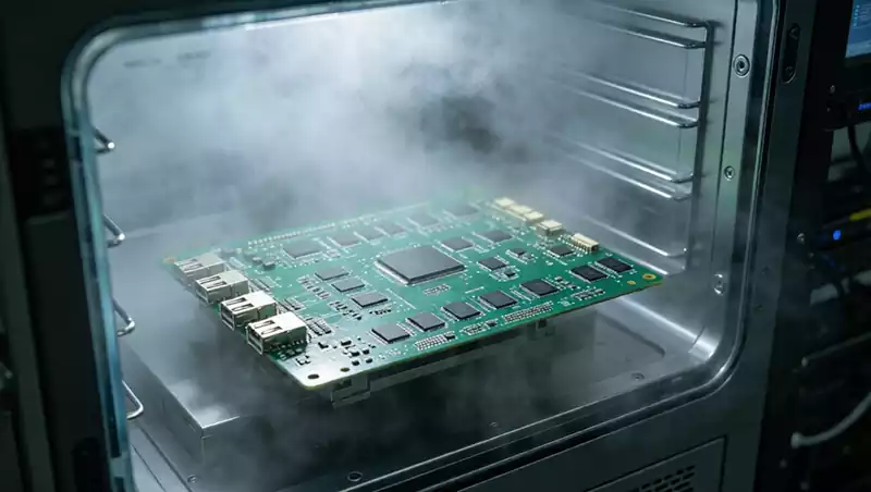
3.Harsh Operating Conditions and Long-Term Reliability Requirements
Data center optical modules often operate continuously in environments reaching 85°C and 85% relative humidity, placing extremely high demands on material stability and structural reliability.
In CPO systems, optical engines and computing chips are tightly integrated, resulting in significantly increased local heat flux density. This requires optical module PCB materials to maintain coefficient of thermal expansion (CTE) control within ±0.8 ppm/°C.
When thermal expansion mismatches occur between PCB substrates and silicon devices, thermal cycling can generate substantial mechanical stress, potentially causing solder joint cracking, trace fractures, and premature product failure.
Long-term exposure to elevated temperature and humidity accelerates material aging. Issues such as dielectric hydrolysis and copper oxidation become increasingly common. Conventional HDI materials often exhibit dielectric constant drift over time, compromising impedance stability.
As a result, high-end optical module PCBs must pass more than 240 hours of thermal cycling and humidity reliability testing before commercial deployment.
Thermal management is equally important. While 400G optical modules already exceed 10 W power consumption, 800G products continue to increase in power density. Consequently, the thermal conductivity of the optical module PCB directly influences long-term operational stability.
4.Increasing Manufacturing Complexity and Cost Pressures
The complexity of high-end optical module PCB manufacturing has increased dramatically, making investments in equipment, advanced materials, and cleanroom facilities key barriers to large-scale production.
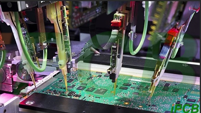
Most high-speed optical module PCBs now rely on modified Semi-Additive Process (mSAP) technology, requiring advanced equipment such as laser direct imaging (LDI) systems and horizontal pulse plating lines. Manufacturing facilities must also comply with Class 1000 cleanroom standards, resulting in significantly higher capital and operating costs than conventional HDI production lines.
Material costs remain another major challenge. Ultra-low-loss laminates such as Panasonic MEGTRON 8 and Rogers RO3000 typically cost three to five times more than standard FR4 materials. Likewise, ultra-low-profile copper foils designed for high-frequency applications further increase production expenses.
Additional factors—including multilayer lamination alignment, contamination control for ultra-fine traces, and micron-level optical alignment requirements—can negatively affect manufacturing yield and increase the cost of each optical module PCB.
Core Optimization Solutions for High-Speed Optical Module PCBs
To address challenges related to signal integrity, routing precision, reliability, and production costs, the industry has established a mature optimization framework encompassing materials, manufacturing processes, and design methodologies.
Advanced Material Systems for Low Loss and High Thermal Conductivity
Material innovation is fundamental to improving optical module PCB performance.
Mainstream ultra-low-loss laminates such as Isola Astra and Shengyi’s SU series can achieve Df values between 0.001 and 0.005, reducing dielectric loss by more than 60% compared with conventional materials.
Modified resin systems with adjustable Dk values ranging from 3.8 to 4.6 enable accurate matching with silicon photonic devices, improving impedance control.
On the conductor side, VLP and HVLP copper foils have become standard for high-frequency designs. Combined with pulse plating technology, these materials effectively mitigate skin-effect-related losses.
For thermal management, metal-core composite substrates and ceramic-filled dielectric materials can increase thermal conductivity from approximately 0.3 W/(m·K) to over 5 W/(m·K). Embedded passive technologies further reduce heat generation by minimizing discrete components.
Manufacturing Evolution from Subtractive to Precision Additive Processes
The widespread adoption of mSAP technology has fundamentally transformed optical module PCB manufacturing.
By combining ultra-thin copper seed layers, photoresist patterning, electroless copper deposition, electroplating, and flash etching, mSAP enables stable mass production of 15 μm line width and spacing structures. The resulting conductor profiles are nearly rectangular, allowing impedance control accuracy within ±3%.
Laser direct imaging systems with 5 μm positioning accuracy replace conventional contact exposure methods, while advanced pulse plating technologies ensure excellent dimensional consistency and copper thickness uniformity.
In heterogeneous integration applications, direct bonding technologies between indium phosphide (InP) lasers and silicon-based PCBs are becoming increasingly mature. Supported by machine vision systems, optical alignment accuracy can reach ±0.1 μm, effectively resolving optoelectronic integration challenges.
Integrated Design Methodologies for Multi-Physics Optimization
Modern optical module PCB development has evolved from traditional circuit design into a multidisciplinary approach incorporating electrical, optical, and thermal engineering.
Three-dimensional layered architectures are increasingly adopted, with optical interfaces on the top layer, high-speed signal routing in the middle layers, and power distribution on the bottom layers.
Gradient microstrip structures ranging from 0.1 mm to 0.15 mm facilitate smooth impedance transitions between silicon photonic devices and PCB interconnects, reducing return loss by up to 8 dB at 56 GHz.
Advanced routing algorithms combined with optical deformation modeling and electromagnetic simulation enable automated optimization of routing paths, significantly shortening development cycles.
Comprehensive verification methodologies—including signal integrity (SI), power integrity (PI), thermal simulation, and electromagnetic compatibility (EMC) analysis—help identify and eliminate potential performance bottlenecks before production.
Technical Advantages and Future Trends of Optical Module PCBs
As computing infrastructure continues to evolve, optical module PCBs are transitioning from simple circuit carriers into highly integrated optoelectronic and thermal management platforms.
Technology Trends
Future optical module PCBs will increasingly incorporate embedded optical waveguides and microfluidic cooling channels, enabling unified integration of optical, electrical, and thermal functions.
Emerging materials such as dynamically tunable dielectric resins and self-healing substrates will further enhance resistance to temperature cycling and humidity exposure.
Hybrid manufacturing technologies combining mSAP and 3D printing are expected to support complex three-dimensional structures while achieving ultra-fine routing capabilities of 10 μm/10 μm required for future 1.6T optical modules.
Application Trends
CPO technology is becoming a major driver of high-end optical module PCB development.
In AI servers and hyperscale data centers, CPO architectures impose significantly stricter requirements. Future optical engine PCBs may exceed 70 layers, require Df values below 0.0015, and maintain CTE tolerances within ±0.5 ppm/°C.
These advancements will substantially increase the value of optical module PCBs compared with conventional server PCBs, creating significant opportunities in high-performance computing markets.
Industry Trends
Digitalization and intelligent manufacturing are reshaping the optical module PCB industry.
Digital twin technologies will enable collaborative simulation of optical modules and PCB systems during development. AI-powered nanoscale visual inspection systems will improve production yield, while integrated optoelectronic testing platforms will simultaneously evaluate signal integrity and optical coupling efficiency.
The industry is also expected to establish unified design and manufacturing standards for high-end optical module PCBs, reducing collaboration costs and improving supply chain efficiency.
The evolution of optical module data rates from 400G and 800G to 1.6T continues to drive fundamental innovation in optical module PCB materials, manufacturing processes, and design methodologies.
Today, ultra-low-loss laminate systems combined with mSAP manufacturing technology have become the industry standard for 800G optical module PCBs. As CPO technology enters large-scale deployment, future optical module PCBs will continue advancing toward higher precision, greater integration, lower signal loss, and superior reliability, providing essential support for next-generation computing networks and high-speed communication infrastructure worldwide.