The Unbreakable “Space Magician”: Deciphering the Microscopic Topology of Double Sided Flexible PCBs
In the demanding battlefield of modern consumer electronics, where the pursuit of “ultra-thinness” and “utilization of irregularly shaped spaces” is fierce, traditional rigid fiberglass circuit boards (such as FR4) are gradually being relegated to secondary roles in many core positions due to their inherent rigidity, weight, and complete inability to bend.
In their place comes a revolutionary type of board material that can be folded, rolled, and even twisted tens of thousands of times under dynamic vibration without signal breakage, much like paper. When such a board needs to be covered with complex integrated circuits on both sides and interconnected through microscopic vias, it becomes the darling of the global high-end supply chain: the double-sided flexible PCB.
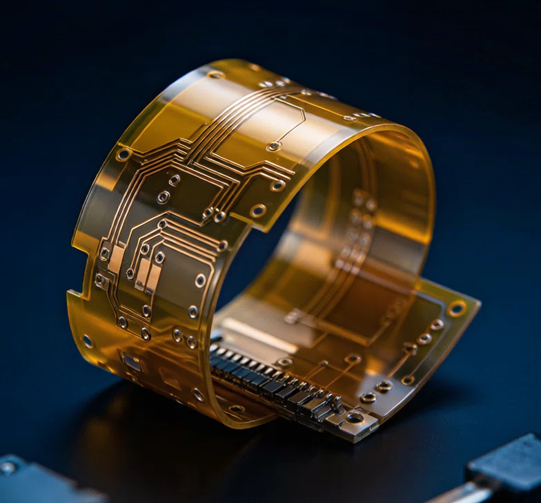
If we were to cut a highly precise double-sided flexible PCB cross-section under a high-powered microscope, we would find that it has completely abandoned the resin and fiberglass cloth upon which rigid boards rely. It is a “microscopic five-layer composite structure” formed by laminating nano-thick polymer insulating films and ultra-thin metal foils through a robust chemical and mechanical process.
Microscopic Physical Anatomy of the Core Five-Layer Structure
Core Insulating Base Film: Located at the very center, this core base is typically made of polyimide (PI) film. This film exhibits a unique translucent amber color and is usually only 12.5 or 25 micrometers thick (equivalent to a fraction of the diameter of a human hair). PI is known as the “king of heat resistance” in the plastics industry, not only remaining undeformed across extreme temperatures ranging from -200 to 300 degrees Celsius, but also possessing remarkable mechanical tear resistance and exceptional electrical insulation properties.
Double-Sided Conductive Copper Foil: Tightly adhered to both sides of the central PI base film are two layers of ultra-thin electrolytic or rolled copper foil. In double-sided flexible PCBs, the thickness of the copper foil is drastically compressed, with the most common specification being one-third of an ounce (approximately 12 micrometers) or even thinner. These two layers of copper foil form the physical carrier for the double-sided circuit traces.
Micro-lamination adhesive layer: Bonding the middle PI base film to the two outer copper foil layers are two layers of modified epoxy resin or acrylic adhesive, only a few micrometers thick. In more advanced “adhesiveless base material” processes, PCB manufacturers even eliminate these two adhesive layers altogether, growing the copper foil directly on the PI surface via vacuum sputtering or hot pressing. This allows for a further 30% reduction in total thickness, resulting in a significant leap in bending life.
Through this ingenious lamination process, double-sided flexible PCBs achieve ultra-high spatial integration with independent wiring on both sides while maintaining a total thickness of approximately 0.1 millimeters.
1.2 The Life-or-Death Battle Between Rolled Copper and Electrolytic Copper: Why Does Choosing the Wrong Material Lead to a “Circuit Break Tragedy”?
A deeply hidden materials science trap: Never use electrolytic copper (ED Copper) in dynamic bending stations; rolled copper (RA Copper) must be used.
Although these two copper foils look identical and are both 99.9% pure copper, their microscopic lattice structures are completely different:
Electrodeposited Copper: It is deposited from a copper sulfate solution using an electrochemical method on a rotating titanium roller. Under a high-powered microscope, its internal lattice exhibits a “columnar crystal structure” perpendicular to the plate surface. This structure resembles rows of vertically standing chopsticks. When a board is subjected to severe horizontal folding and bending, stress concentration occurs instantly in the gaps between the chopsticks, causing lattice cracks to split vertically. After dozens of bends, the traces will undergo catastrophic microscopic brittle fracture.
Rolled Annealed Copper: This is produced by repeatedly rolling, stretching, and thinning a thick copper block hundreds or thousands of times using massive heavy-duty mechanical rollers, followed by high-temperature annealing. Under immense mechanical force, its internal lattice is completely reshaped into a “layered, flat, fish-scale structure” parallel to the board surface. This lattice is like a stack of deck of cards. When the board bends, the cards can slip and misalign microscopically, greatly distributing the mechanical stress. Double-sided flexible circuit boards made with rolled copper can withstand 200,000 folds at the hinge of a foldable phone without any impedance drift. This is the technological moat of a top-tier supply chain.
Micro-via plating and blind via routing: The unique “microscopic tunnel” hell of flexible PCBs
Since double-sided flexible PCBs have independent wiring on both the front and back layers, in order for the control signals on the front to direct the driver chips on the back, we must create a series of electrical interconnection “microscopic underground tunnels” between the two copper foil layers. This seemingly simple drilling and plating process in rigid boards becomes a nightmare for field process engineers (PEs) in the world of flexible films.
The precision showdown between mechanical punching and UV laser drilling
In traditional FR4 rigid boards, we can easily drill holes with a diameter of 0.2 mm using a high-speed mechanical alloy drill bit, like a drilling machine, with a simple pull and pull motion. However, on the PI substrate, which is only tens of micrometers thick and as soft as paper, once the mechanical drill bit plunges downwards at high speed, the enormous shearing force causes the soft PI film to instantly undergo severe “tearing, stretching, and burr” deformation, resulting in holes with edges that look like they’ve been chewed by a dog.
Therefore, modern double-sided flexible printed circuit board (PCB) hole processing has increasingly relied on ultraviolet (UV) laser drilling technology.
A high-energy UV laser beam is focused into a microscopic spot with a diameter of only 50 micrometers (or even smaller), bombarding the board surface at an astonishing rate of thousands of holes per second. Due to the “photoablation” property of UV lasers, it relies on high-energy photons to directly shatter the polymer chemical bonds within the polyimide (PI), causing the material to vaporize instantly without generating any mechanical stress.
However, the biggest challenge of laser drilling lies in Joule heating control and slag removal.
The instant the laser burns through the upper copper layer and penetrates the intermediate adhesive layer and PI layer, the locally generated high temperature causes the modified epoxy resin adhesive to instantly melt microscopically, turning into a sticky, highly carbonized black “resin smear” that stubbornly adheres to the inner walls of the entire underground tunnel. If this layer of insulating black adhesive residue is not completely removed, the copper plating process will be blocked by the residue, creating a serious “open circuit” or breaking completely due to thermal expansion during use.
Vertical Continuous Plating (VCP) and the “Skeleton Support” Art of Flexible Circuit Boards
To clean the tunnel, the PCB manufacturer must send the flexible circuit board into a highly oxidizing “adhesive residue removal tank” composed of high-concentration potassium permanganate for microscopic chemical cleaning. After cleaning, the next step is the copper plating process, which connects the copper foil at both ends of the tunnel.
Ordinary rigid circuit boards, due to their rigid skeleton, can remain motionless under the high-pressure spray of chemicals in the plating tank. However, flexible circuit boards, being extremely thin and soft, will violently shake, twist, and be attached like a kite in the turbulent liquid once they are hung on the plating rack and sent into the plating tank. This results in extremely uneven current density across the entire board. Some areas inside the holes are plated with thick copper, while others, due to the vibration, are in “current dead zones,” creating fatal plating voids.
To overcome this process defect, high-end flexible PCB manufacturers must mandate the use of a vertical continuous plating (VCP) system specifically designed for flexible PCBs on their production lines.
Before the board enters the plating tank, its top, bottom, left, and right edges are tightly gripped and forcibly stretched by specially designed precision metal clamps with high-tension springs, taut the entire flexible board into a rigid plane as hard as a drumhead.
Simultaneously, the chemical spray nozzles inside the plating tank employ an extremely sophisticated symmetrical balanced fluid dynamics design, ensuring that the pressure of the plating solution flowing from the front and back cancels each other out microscopically. Through this perfect synergy of fluid dynamics and electrochemistry, high-purity copper ions can be stacked uniformly and smoothly on the inner wall of laser-guided holes with diameters of only tens of micrometers, creating absolutely robust, zero-void double-sided conductive micro-tunnels.
The Physical Balance of Dynamic Bending: The Mechanical Game Between Neutral Axis Theory and Coverlay
Once double-sided traces and micro-via connectivity are achieved, a double-sided flexible PCB possesses complete electrical functionality. However, for long-term industrial applications, it must pass the ultimate mechanical test: how to ensure that the outer copper traces do not undergo microscopic fatigue cracking during long-term dynamic folding?
In the mechanical design of flexible PCBs, this follows a supreme golden law of physics—the Neutral Axis theory.
Microscopic Tearing in the Bending World: What is a Neutral Axis? When you take a piece of thick cardboard and fold it forcefully, you can clearly observe a physical phenomenon: when the cardboard is folded and bent, the paper fibers near the outer edge are forcibly stretched and torn, while the paper fibers near the inner edge are strongly compressed and wrinkled.
Between these two diametrically opposed tensile and compressive stresses, there must exist a very special microscopic geometric cross-section with zero thickness. At this cross-section, the material is neither subjected to any tension nor compression; its internal stress is perfectly zero. This absolutely safe stress dead angle is called the neutral plane in the mechanics of materials.
For double-sided flexible printed circuit boards (FPCBs), they have two layers of copper foil. When we bend the entire FPCB, one layer of copper foil on the outer edge is subjected to tensile stress, while the other layer on the inner edge endures compressive stress. Because copper is a ductile material but highly susceptible to metal fatigue, if the two layers of copper foil deviate too far from the neutral plane, after hundreds of thousands of repeated stretching and compression, the outer copper traces will instantly crack with countless microscopic, fatal microcracks, much like repeatedly folded iron wire.
Coverlay Mechanical Fine-Tuning: Ensuring Copper Traces Perfectly Stay Within the Safe Zone
To extend the bending life of double-sided flexible circuit boards (FPCBs), manufacturers cannot use ordinary solder mask as they do with rigid boards. Rigid solder mask is extremely brittle and will flake off like shattered glass with a single bend. FPCBs must use a dedicated protective layer—a flexible insulating coverlay.
The coverlay is also composed of a PI substrate and special adhesive. During the final assembly stage, the manufacturer uses a high-temperature hot press to firmly press the coverlay onto the etched double-sided traces.
Here, the coverlay not only provides electrical protection through insulation and moisture protection, but it also acts as a powerful mechanical center of gravity adjuster.
Experienced structural engineers perform “symmetrical geometric fine-tuning” by precisely calculating the thickness of the top cover film, the thickness of the intermediate base film, and the mechanical modulus of the adhesive layer: If the thickness of the top and bottom cover films are made absolutely identical, and the intermediate base film is centered, then according to the principle of mechanical equilibrium, the overall mechanical neutral plane of this double-sided flexible PCB will be precisely “forced” to the center, sandwiched exactly between the insulating PI layer and the two ultra-thin copper foils.
Although the copper foils cannot perfectly overlap the neutral plane, due to the overall symmetrical design, the physical distance between the two copper foil layers and the neutral plane is compressed to its limit (typically only a few micrometers). This means that when the board bends, the tensile and compressive stresses borne by the two copper foil layers are reduced by more than 90%. The copper atoms are thus safely housed in a low-stress zone, achieving the remarkable lifespan of hundreds of thousands of folds without breaking a sweat.
The “Golden Hub” of the Global Precision Folding and New Energy Intelligent Supply Chain
As human technology fully embraces the era of 5G intelligence, wearables, and green transportation, double-sided flexible PCBs have completely transcended their early marginal role. They are no longer just simple jumpers, but constitute the golden hub of the global supply chain for precision folding terminals, high-energy sensors, and new energy batteries.
Dominating Two Super Tracks that Will Change the Future
In the current and future industrial supply chain landscape, double-sided flexible PCBs firmly hold two irreplaceable entry tickets:
Foldable Phones & Ultimate Wearables (Foldable Devices & AR/VR): Foldable phones can function as tablets when unfolded and phones when folded. The hinge, with its narrow gap connecting the left and right motherboards, is made of a custom-designed double-sided flexible PCB. It must be densely packed with hundreds of high-speed differential signal lines, transmitting 4K high-definition screen signals while enduring dozens or even hundreds of relentless folds by users every day. In AR/VR glasses, to reduce weight to the gram level, all internal sensors and camera connections are made using a double-sided flexible circuit board laid around the curved surface of the human face.
New Energy Vehicle Battery Management System (BMS FPC): Inside the massive battery packs of modern smart electric vehicles like Tesla and BYD, hundreds of lithium-ion battery cells require real-time monitoring of voltage and temperature. Traditionally, this requires hundreds or even thousands of bulky, inefficient, and easily short-circuited copper wires due to vibration and wear. Modern high-end battery packs, however, use a single, several-meter-long custom double-sided flexible circuit board. It is directly mounted on top of the battery array, with the acquisition chip and explosion-proof fuse soldered to the front and an insulating layer on the back. This thin, lightweight board replaces the entire vehicle’s bulky wiring harness, not only reducing the vehicle’s weight by tens of kilograms and increasing range, but also achieving a significant leap in battery pack production yield through automated, fully bonded assembly.
Adhesiveless Requirement: For ultra-thin, dynamically foldable applications such as medical endoscopes, this standard mandates the use of adhesive-free double-sided substrates (such as DuPont Pyralux series or equivalent Grade A materials) to eliminate the risk of delamination caused by adhesive layer aging.Surface Finish Fine-tuning: Because flexible circuit boards (FPCBs) are highly susceptible to blistering due to moisture absorption during soldering, it is crucial to specify whether electroless nickel-gold (ENIG) or gold plating is used for the surface finish. The gold layer thickness must be precision-grade (typically no less than 2 microinches) to ensure excellent yield rates for both manual placement and automated reflow soldering.
Customized Stiffener Integration: While FPCBs prioritize flexibility, FR4 or polyimide (PI) reinforcing sheets must be added locally in the interface areas where components and chips need to be mounted. This localized rigidity reinforcement ensures that chip leads will not deform or peel off under external insertion and extraction forces, achieving the highest quality delivery that balances rigidity and flexibility.