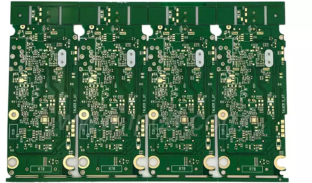
Underetching of PCB circuit traces primarily occurs during the etching process. Any deviation in the concentration, temperature, spray pressure or etching time of the etching solution will significantly increase the risk of underetching.
Many PCB manufacturers encounter underetching issues because they adopt a ‘one-size-fits-all’ approach to parameter settings, failing to take into account the differing etching requirements of varying trace widths and copper foil thicknesses. This results in some traces being over-etched, causing the underside to be eroded.
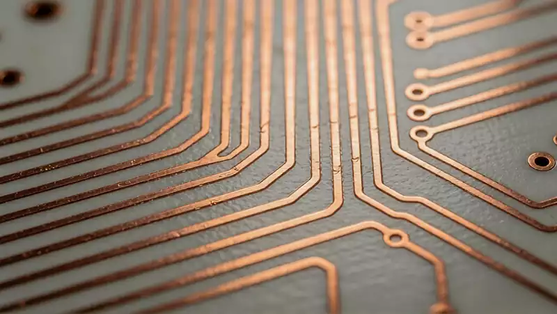
Control of PCB Etching Process Parameters
Maintaining a stable concentration of the etching solution is fundamental. Whether using acidic copper chloride or alkaline ammonium copper etching solutions, excessively high concentrations increase etching activity and accelerate lateral etching; conversely, excessively low concentrations prolong etching time and similarly exacerbate undercutting. In practice, concentration standards should be tailored to the thickness of the copper foil: for example, the specific gravity range of the acid etching solution suitable for 18μm thin copper foil is 1.20–1.30, whilst for 35μm thick copper foil, the concentration must be appropriately reduced. Additionally, an automatic hydrometer and pH meter should be provided, with spot checks conducted hourly to promptly replenish oxidants or diluents, ensuring concentration fluctuations remain within permissible limits.
Temperature control is equally critical. As etching is an exothermic reaction, the etching rate nearly doubles for every 10°C increase in temperature; excessive heating significantly enhances the lateral corrosion capability of the etching solution. Typically, the temperature for acid etching is maintained between 45 and 50°C, and for alkaline etching between 45 and 55°C. A temperature control warning system should be installed to prevent localised overheating that could lead to over-etching.
Optimising spray pressure and angle is a key detail in avoiding undercut. In mainstream spray etching processes, nozzle blockages or uneven pressure can cause inconsistent impact of the etchant on the circuit surface: excessive pressure tends to impact the circuit edges, exacerbating undercut; insufficient pressure fails to thoroughly etch away excess copper foil, thereby requiring extended etching times and indirectly increasing the risk of undercut. It is recommended to maintain spray pressure between 1.5 and 2.5 bar, clean the nozzles regularly to ensure consistent spray angles across all nozzles, and prioritise vertical spraying to enhance the vertical etching capability of the solution and minimise lateral erosion.
Etching time should be controlled in conjunction with test etching results, adjusting the conveyor speed according to circuit width and copper foil thickness. For example, for 0.1 mm fine lines and 18 μm copper foil, etching time should be controlled between 60 and 80 seconds to avoid bottom over-etching caused by excessive dwell time. Additionally, install automatic end-point detection equipment to monitor etching progress in real time and prevent over-etching.
Resist Quality and Pretreatment
The photoresist acts as a ‘protective shield’ for the circuit lines; its quality directly determines whether the etchant will penetrate the underside of the lines and cause over-etching. Many companies neglect the control of the photoresist, for example by selecting low-resolution photoresist materials, or failing to carry out thorough pre-treatment, resulting in insufficient adhesion of the photoresist. During etching, the edges of the photoresist may lift or develop voids, allowing the etchant to seep in and erode the underside of the lines laterally, forming over-etching defects.
The selection of photoresist materials must align with production requirements. For fine-line PCBs, high-resolution dry films or liquid photoresists (LPI) should be prioritised, with a resolution of no less than 20 μm. After development, the edges must be free of burrs and defects to ensure a tight seal against the copper foil surface, thereby blocking the penetration path of the etching solution. If electroplated tin or tin-lead layers are used as the resist layer, the plating must be dense and free of pores to prevent the etchant from seeping through the pores to the underside.
The refinement of the pretreatment process is equally important: The substrate must undergo thorough degreasing and roughening, with micro-etching depth controlled between 1.0 and 1.5 μm to enhance the adhesion between the resist layer and the copper foil; a pre-baking step should be added prior to etching to further cure the resist layer, thereby preventing delamination or lifting during etching.
Control of the Development Process
Control of the development process is equally crucial. Excessively high developer concentration or prolonged development time can damage the edges of the resist layer, causing blurred edges and providing an opportunity for lateral etching by the etchant; conversely, incomplete development leaves residual resist, affecting the etching outcome. In practice, the developer concentration should be maintained between 0.8% and 1.2%, with development time adjusted according to the type of resist layer. Thorough rinsing must be carried out after development to ensure no developer residue remains, thereby preventing any impact on the protective performance of the resist layer and reducing the likelihood of etchant penetration at source.
Material Selection and PCB Design
The occurrence of undercut on the underside of the circuit is not only related to process control; the choice of materials and the rationality of the PCB design also directly influence the level of undercut risk. Unsuitable material selection and design can create underlying risks of undercut from the outset; even with rigorous subsequent process control, these risks are difficult to eliminate entirely.
The choice of copper foil thickness must be matched to the circuit precision. The thicker the copper foil, the longer the etching time required, and the higher the risk of lateral etching. For fine-line PCBs, excessive use of thick copper foil significantly increases the probability of undercut. It is recommended that ultra-thin copper foil (12–18 μm) be prioritised for precision circuits to reduce etching volume and minimise the risk of lateral etching.
If thick copper foil must be used, the semi-additive process (mSAP) or modified subtractive process may be employed to reduce lateral etching during the etching process. Careful consideration must also be given to the choice of substrate. Substrates with high surface flatness and strong adhesion should be prioritised to prevent over-etching caused by poor adhesion of the resist layer due to surface irregularities.
Optimising PCB design can reduce the risk of over-etching at source. For fine-line designs, particular attention must be paid to line width compensation: the design line width should be widened in advance according to the etching factor, typically by 5–10 μm, to offset losses during the etching process, prevent the line width from becoming too narrow after etching, and simultaneously mitigate the impact of bottom over-etching. The routing direction must also be optimised to avoid parallel alignment between the traces and the flow of the etchant; vertical routing should be prioritised to reduce the continuous impact of the etchant on the edges of the traces.
Rounded corners should be incorporated at trace junctions to prevent the accumulation of etchant at these points, which can lead to localised over-etching. Furthermore, pcb trace spacing should be carefully controlled during design to prevent overly narrow gaps that could impede the flow of the etchant, thereby exacerbating localised over-etching.