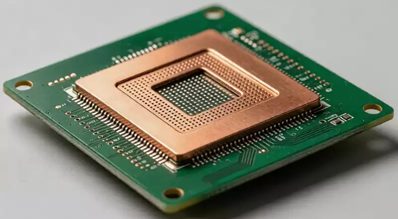
Thanks to their high detection accuracy, strong interference resistance and high resolution, 77GHz millimetre-wave radars pcb are widely used in fields such as autonomous driving, smart security and driver assistance systems. As the core component responsible for signal transmission, current-carrying and heat dissipation, as well as structural support, the high-frequency transmission performance, copper thickness precision and structural stability of radar PCBs directly determine the detection accuracy and service life of millimetre-wave radars.
Compared to standard PCBs, 77GHz millimetre-wave radar PCBs impose extremely stringent manufacturing requirements regarding high-frequency low-loss transmission, current-carrying capacity, and overall thermal dissipation performance. To balance the dual core requirements of ultra-low signal loss in the radar antenna area and high current-carrying capacity coupled with robust thermal dissipation in the non-antenna functional areas, the industry generally adopts a differentiated structural design featuring thin copper in the antenna area and thick copper in the non-antenna areas.
Preliminary Material and Design Preparation (Process Fundamentals)
1.Selection of Composite Substrates
High-frequency, low-loss hybrid composite substrates are utilised to achieve the optimal balance between radar PCB performance and cost. The top-layer antenna-dedicated layer utilises Rogers RO3003 or RO4835 series, or domestically produced ceramic-filled PTFE high-frequency substrates of equivalent grade. Key parameters are strictly controlled: dielectric constant Dk = 3.48 ± 0.05 and loss factor Df ≤ 0.004, to minimise signal transmission loss at 77 GHz and ensure radar detection accuracy.
The bottom layer and non-antenna functional inner layers utilise standard FR-4 substrate. Leveraging its excellent structural rigidity and cost-effectiveness, this ensures the overall structural stability and mechanical strength of the radar PCB. Layers are bonded using specialised, high-stability prepregs, with precise control over lamination temperature and pressure parameters to eliminate defects such as delamination, interlayer misalignment and bubbling. This ensures structural consistency in the multilayer board, making it suitable for long-term use in complex operating conditions.
2.Selection of Reference Copper Foil
The entire board utilises HVLP (Ultra-Low Profile) copper foil. Its extremely low surface roughness suppresses high-frequency skin effect losses at source, perfectly matching the transmission characteristics of 77 GHz millimetre-wave high-frequency signals. It is the core material for ensuring the high-frequency, low-loss performance of the radar PCB.
The initial reference copper foil thickness is set at 10±1μm, allowing ample margin for chemical thinning and selective plating adjustments. This effectively mitigates the accumulation of deviations in initial copper thickness, ensures controllable process precision for subsequent zone-specific copper thicknesses, and lays the foundation for the manufacture of differentiated copper thickness structures.
2.Standardisation and Verification of Design Files
Close coordination with the design team is undertaken in advance to conduct a dedicated review of Gerber files. The radar PCB is clearly divided into two main functional copper zones, with defined process standards for each: the target thickness for the antenna thin-copper area is 28±5 μm, ensuring lossless high-frequency signal transmission.
The target thickness for the non-antenna thick-copper functional area is 48±8 μm, meeting the requirements for high current carrying capacity and rapid heat dissipation. All zone boundaries are individually marked and precisely positioned to eliminate issues such as blurred boundaries and cross-contamination between zones.
Simultaneously, clearly define the board-wide impedance control tolerance of ±5%, as well as the core parameters for blind and through-holes (diameter, position and depth). Provide a comprehensive process specification document that clearly outlines special process requirements for each zone, such as plating, pattern formation and solder mask openings, to ensure precise implementation of process standards on the production side. This completely eliminates any disconnect between design and manufacturing, guaranteeing consistency in the mass production of radar PCBs.
Core Mass Production Manufacturing Processes
Step 1: Precision Cutting of Substrates and Pre-treatment for Differential Drilling
The core objective of this process is to finalise the substrate shape and achieve precise machining of interlayer vias, whilst avoiding defects such as drilling damage and dust residue on the hole walls, thereby laying a solid foundation for subsequent via metallisation and multi-layer interconnection.
First, precision cutting of the substrate is carried out, with high-frequency substrates and FR-4 substrates processed strictly in accordance with the radar PCB’s dimensional specifications. The edges are finely sanded to remove burrs and flash, with dimensional tolerances strictly controlled to ≤±0.1mm to ensure compatibility for subsequent assembly.
Drilling employs a differentiated, step-by-step process of “laser processing for blind vias and mechanical processing for through-holes” to accommodate the structural characteristics of different areas: Micro-blind vias connecting the antenna layer to internal layers are processed using laser drilling equipment, with hole diameters stably controlled to the 0.1 mm level and drilling depth accuracy of ±5 μm, ensuring the interlayer connectivity precision and signal integrity of the radar PCB’s high-frequency circuit layers.
Large-diameter through-holes in non-antenna areas are produced using mechanical drilling to avoid substrate deformation and performance deviations in thick copper regions caused by thermal damage from laser processing.
Following drilling, a dual-process of high-pressure water washing and mechanical polishing is employed to thoroughly remove dust from the hole walls and burrs from the edges, thereby eliminating the risk of voids in the hole walls or plating peeling during the subsequent copper plating process. Finally, a hole-wall activation pre-treatment is carried out, comprising substrate roughening, resin removal and activation.
The roughening process creates a microscopic rough surface on the hole walls to enhance copper layer adhesion; the activation process uniformly adsorbs palladium catalyst particles onto the hole walls, providing stable catalytic conditions for chemical copper plating and ensuring continuous, full coverage of the conductive film on the hole walls.
Step 2: Dual-Layer Via Metallisation Process (Electrolytic Copper Plating + Via Filling)
Via metallisation is a critical process for ensuring the reliability of electrical continuity in multi-layer radar PCBs. This paper adopts a two-step process comprising ‘electrolytic copper plating as a base layer followed by precision via filling and thickening’, which balances the flatness of blind via filling with the consistency of copper conductivity across the entire board, effectively avoiding critical defects such as interlayer open circuits and poor contact.
The first step involves chemical copper plating: the pre-treated substrate is immersed in a precisely formulated copper plating solution (a system comprising copper sulphate, formaldehyde and complexing agents). Through an autocatalytic redox reaction, a uniform, thin conductive copper film of 0.3–0.5 μm is deposited on the hole walls and the board surface, achieving complete electrical conductivity of the hole walls and establishing a complete electrical pathway for subsequent plating.
During the process, the temperature, concentration and pH of the solution are dynamically monitored in real time to ensure the copper film is free from breaks, voids and bare spots, thereby guaranteeing stable basic conductivity.
The second step involves specialised plating for filling blind vias: the plating current density is maintained at a stable 14–16 ASF. By employing a low current density mode, excessive thickening of the copper layer on the board surface is effectively minimised, whilst improving the uniformity of the copper layer. Upon completion of the plating process, the fill depth of the blind vias fully meets the specifications, and the base copper thickness across the entire board is uniformly increased to 45±4 μm, providing ample margin for subsequent precise micro-adjustments to the copper thickness in specific zones of the radar PCB.
Step 3: Full-board chemical thinning to standardise the copper thickness
To address minor variations in copper thickness on the board surface following via-filling plating, a full-board chemical thinning process is employed to standardise the reference thickness of the Radar PCB, thereby eliminating the impact of initial thickness variations on the precision of the finished product. A specialised copper-stripping solution based on a sulphuric acid-hydrogen peroxide system is employed, with standard concentrations of: 100–180 g/L sulphuric acid, 20–40 g/L hydrogen peroxide, and 0–50 g/L copper ions. The process is conducted at a constant temperature of 30–35°C, utilising a spray-coating method to ensure uniform copper reduction across the board surface.
Copper thickness data is monitored in real-time during the process, with the final copper thickness across the entire board reduced to 20±5 μm, and the variation in copper thickness across the board surface controlled within 5 μm, ensuring uniform thickness throughout. Upon completion of the reduction process, the boards are thoroughly rinsed with deionised water to completely remove any residual chemical solution from the surface.
They are then placed in a drying oven at 80–100°C for constant-temperature drying to eliminate any residual moisture or chemical solution, providing a high-precision, contamination-free substrate for subsequent dry film lamination and electroplating processes.
Step 4: Through-hole Reinforcement Plating to Finalise the Thin Copper Antenna Layer
First, a secondary electroless copper plating process is carried out on the machined through-holes to precisely repair microscopic damage to the hole walls caused by the drilling process. This ensures highly consistent continuity of the copper layers in the radar PCB’s through-holes and blind vias, guaranteeing stable and reliable electrical interlayer connectivity across the entire board and preventing signal interruptions or poor contact during high-frequency operation.
Subsequently, a full-board flash plating operation is carried out. Through a short, precise electroplating process, the copper thickness in the antenna area of the radar PCB is accurately increased to the design standard of 28±5μm, thereby finalising the formation of the thin copper antenna layer. At the same time, plating parameters are strictly controlled to ensure that the copper thickness in all through-holes is consistently maintained within the acceptable range of 18–35μm.
Electroplating current uniformity is monitored throughout the process to eliminate deviations in copper thickness within the antenna area and localised thickness inconsistencies, thereby guaranteeing the integrity and stability of 77 GHz high-frequency signal transmission at the process level.
Step 5: Selective pulse electroplating to achieve thick copper in non-antenna areas
This process is central to realising the radar PCB’s differentiated zoning structure of ‘thin copper for the antenna and thick copper for functional areas’. Through a combined process of dry film masking and selective pulse electroplating, we precisely achieve differentiated copper thickness processing across zones, completely eliminating mass production defects such as cross-plating and boundary shifts.
First, vacuum dry film lamination is performed. Using vacuum lamination equipment, the dry film is tightly bonded to the copper layer on the board surface, completely eliminating bubbles, wrinkles and gaps in the bond to ensure effective masking protection. This is followed by precise exposure using LDI (Laser Direct Imaging) equipment, which cures the dry film only in the antenna areas. After development, only the non-antenna areas requiring thickening are exposed. The exposure positioning accuracy reaches ±10–15 μm, ensuring that the boundaries between thick and thin copper zones are neat, without misalignment or blurring.
Secondly, a pulse electroplating process is employed to thicken the exposed non-antenna functional areas. By precisely controlling the plating current and duration, the copper thickness in these functional areas is consistently increased to the target standard of 48±8μm. Specialised levelling agents and brighteners are added to the plating solution to optimise the copper layer deposition structure, resulting in a dense grain structure and a smooth surface for the thick copper layer.
This significantly enhances the current-carrying capacity and heat dissipation performance of the radar PCB, making it suitable for high-load continuous operation scenarios. In the antenna areas masked by the dry film, no copper is deposited, and the thin copper layer maintains a constant thickness.
Following electroplating, a specialised film-stripping solution is used to completely remove the dry film from the antenna areas, ensuring the board surface is free of residues and adhesive stains, thereby clearing the way for subsequent precision pattern etching processes.
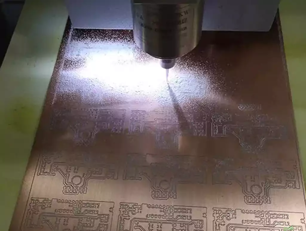
Step 6: High-precision pattern etching to form the antenna and circuit structures
To address the height differences between thick and thin copper zones on radar PCBs, we have innovatively adopted a secondary precision dry film imaging process. This completely resolves imaging defects caused by height variations and ensures high-precision pattern transfer. A dry film is vacuum-bonded to the entire board, utilising the film to fill the gaps at the interface between thick and thin copper layers, thereby eliminating issues such as imaging gaps and ghost edges.
Subsequently, LDI laser imaging equipment is used to precisely transfer the antenna patterns and functional circuit patterns onto the dry film layer; after development, the areas of excess copper to be etched are precisely exposed.
Precision etching is carried out using vacuum etching equipment. Etching parameters and chemical ratios are continuously optimised, and etching factors are strictly controlled to minimise side-etching effects. Upon completion of etching, the antenna edges are steep and straight, free from burrs and residual copper, with line width tolerances consistently maintained within ±10–15 μm.
The etching process is monitored in real time throughout to precisely avoid issues such as antenna pattern damage caused by over-etching or copper residue resulting from under-etching. After etching, the entire dry film is stripped away, revealing a complete thin-copper antenna pattern and a thick-copper non-antenna circuit structure.
Step 7: High-frequency-optimised surface anti-oxidation treatment
Given the transmission characteristics of 77 GHz high-frequency signals, the use of the electrochemical nickel-gold (ENIG) process is strictly prohibited for radar PCBs. The magnetic properties of nickel induce high-frequency hysteresis losses, significantly attenuating signal strength and severely compromising the detection accuracy and stability of millimetre-wave radar.
This paper recommends the low-loss electroless silver plating process as the primary surface treatment solution. It offers core advantages of excellent conductivity, high surface flatness and extremely low high-frequency loss, making it perfectly suited to the high-frequency operational requirements of radar PCB antenna areas.
Alternative processes can be flexibly selected for different application scenarios: the electroless tin plating process offers good flatness and is suitable for conventional assembly scenarios; the OSP (Organic Solderable Phosphate) process offers the lowest high-frequency loss but has relatively weaker oxidation resistance, making it suitable for products requiring short-term storage or rapid mass production.
Throughout the surface treatment process, core parameters such as chemical solution temperature and immersion duration are strictly controlled to ensure the coating uniformly covers the entire copper surface, with consistent thickness, no missed plating and no build-up. This approach balances copper layer oxidation protection, lossless high-frequency signal transmission and the reliability of subsequent component soldering.
Step 8: Differentiated Solder Mask Process, Antenna Area Window Protection
A screen printing process is used to uniformly apply green or red solder mask ink onto the radar PCB surface, with precise control over coating thickness to eliminate defects such as bubbles, pinholes and uneven thickness. Through a precise exposure and development process, the high-frequency antenna areas are fully exposed, completely removing the solder mask ink from these regions to expose the functional plating layer; the non-antenna functional areas retain a complete solder mask layer, fully utilising its role in insulation, isolation, oxidation prevention, protection against solder short circuits, and wear resistance.
The antenna area is strictly kept free of any solder mask residue to prevent the dielectric properties of the ink from interfering with the normal propagation of electromagnetic waves, thereby eliminating performance issues such as deviations in radar detection accuracy and signal attenuation. Finally, the board is placed in a curing oven, where the solder mask is cured at a constant temperature of 150–160°C.
This ensures a strong bond between the ink, the substrate and the copper layer, guaranteeing long-term performance stability and suitability for complex automotive and industrial operating environments.
Step 9: Contour Shaping and Comprehensive Final Inspection
Using CNC milling or laser cutting processes, the final contour shaping of the radar PCB is completed in strict accordance with the design drawings. Excess substrate material is precisely removed from the edges, with dimensional tolerances controlled within ±0.1 mm. Following cutting, the edges are finely polished to remove burrs, ensuring the compatibility and consistency of the complete product assembly.
Comprehensive specialised performance testing is conducted, with core test items including: impedance testing (tolerance ±5%), interlayer continuity testing, and insulation performance testing. Special attention is given to verifying the transmission loss of 77GHz high-frequency signals in the antenna region to ensure full compliance with millimetre-wave radar performance standards.
Simultaneously, the copper thickness in each section is inspected board by board to verify that the thin copper in the antenna area and the thick copper in the functional areas meet specifications, and that the uniformity of copper thickness across the board surface complies with mass production standards.
Combining visual inspection with microscopic examination, we comprehensively screen for surface defects such as scratches, bubbles, residual copper and solder mask peeling, whilst verifying the integrity of antenna patterns and the clarity of boundaries between thick and thin copper zones, thereby eliminating defective products with misaligned patterns or blurred boundaries.
Non-conforming products are categorised for repair; those beyond repair are uniformly scrapped to guarantee the quality of products leaving the factory. Qualified products are vacuum-sealed to prevent moisture ingress, oxidation and impact damage during transport and storage. Product model, production batch and date of manufacture are clearly marked, ensuring standardised delivery upon dispatch.
Key Process Control Points
1.Precise Control of Copper Thickness in Different Zones
A closed-loop copper thickness monitoring system is established to cover the entire process, encompassing all stages from the initial copper foil incoming inspection, via-filling plating, global thinning, antenna zone shaping plating, to selective thickening in functional zones. A system of batch sampling combined with 100% inspection at critical workstations is implemented to track changes in copper thickness data throughout the process.
Strictly ensure that copper thickness in both antenna and non-antenna zones meets specifications, with board-level copper thickness uniformity within ≤5μm, thereby eliminating issues such as abnormal signal impedance, insufficient current-carrying capacity and uneven heat dissipation caused by localised copper thickness deviations.
2.Control of Pattern and Zone Positioning Accuracy
We uniformly control the exposure accuracy of LDI laser imaging to ≤±10–15 μm. Combined with a vacuum dry film lamination process, this completely eliminates defects such as bubbles, misalignment and creases in the film. This ensures that the boundaries between thick and thin copper zones on radar PCBs are regular, and that antenna patterns are free from misalignment and distortion, thereby consistently achieving precise high-frequency impedance matching and meeting the dual design requirements of current-carrying capacity and signal integrity.
3.Quality Control of Via Plating
Strictly adhere to standardised parameters throughout the entire process of immersion copper plating and via-filling electroplating to ensure continuous, full coverage of the via walls with no voids or breaks; Precise regulation of plating current density and duration for via filling maintains blind via depression within acceptable limits, ensuring uniform copper layer thickness in both through-holes and blind vias, thereby eliminating critical quality defects such as interlayer electrical failure and plating peeling from the outset.
4.Dedicated Control of High-Frequency Performance
Strictly enforce admission standards for high-frequency substrates to prevent the use of materials that fail to meet the required dielectric constant and loss factor specifications; Prohibit the use of magnetic metal surface treatment processes throughout the entire process to safeguard the core characteristics of high-frequency, low-loss radar PCBs; ensure that solder mask openings in the antenna area are completely free of residue, strictly control the side etch rate during the etching process, guarantee the regularity of antenna edge structures, minimise signal transmission loss at 77 GHz, and meet the high-precision and high-sensitivity detection requirements of millimetre-wave radar.
Core Process Advantages and Mass Production Considerations
1.Core Process Advantages
The radar PCB mass production process developed in this paper innovatively adopts a manufacturing approach of “uniform base thickness combined with zone-selective thickening”, thoroughly resolving the industry pain points associated with traditional step-by-step thinning processes, such as uneven copper thickness, poor stability and low yield rates. Leveraging core technologies such as LDI high-precision imaging, pulse-selective electroplating, differential drilling, and high-frequency-optimised surface treatment, the process precisely realises a differentiated zoned structure featuring thin copper for the antenna and thick copper for functional areas.
This simultaneously addresses the multiple requirements of high-frequency, low-loss transmission performance in the antenna zone and high current-carrying capacity, strong heat dissipation, and high structural stability in the functional zones.
The step-by-step via metallisation process significantly improves the quality of blind via filling and the consistency of through-hole conductivity, effectively enhancing product yield and batch stability. The complete process is perfectly suited to the mass production of 77GHz millimetre-wave radar PCBs. It enables precise control over key metrics such as impedance control, signal integrity and partition structure accuracy, whilst striking a reasonable balance between product performance and production costs. With its strong practicality and suitability for mass production, it can be widely applied to various high-frequency radar devices, including automotive millimetre-wave radars, industrial detection radars and security radars.
2.Mass Production Considerations
High-frequency substrate management: Rogers series substrates and domestic high-frequency substrates of equivalent grade must be stored in sealed containers throughout the process. Strict control of temperature and humidity in both storage and production environments is required to prevent moisture ingress, dust accumulation and contamination, thereby avoiding shifts in dielectric parameters and reduced copper layer adhesion. This ensures the stability of the radar PCB’s high-frequency performance from the material stage.
Process Chemical Management: For core process chemicals such as copper plating, electroplating, copper stripping and etching, a mechanism for regular testing and replacement must be established. The concentration, temperature and pH of the solutions must be monitored in real time, with ratios adjusted promptly to avoid process defects such as uneven plating, etching residues and poor copper layer adhesion caused by chemical ageing or deterioration.
Production Environment Control: The entire process must be carried out in a Class 1000 or higher cleanroom, with a constant ambient temperature of 23±2°C and humidity of 45±5%. This effectively isolates dust and impurity contamination, significantly reducing the probability of surface defects and performance anomalies in radar PCBs, and ensuring batch product consistency.
Design and Process Coordination: Prior to mass production, in-depth two-way coordination between design and process teams must be completed to clarify core requirements such as the boundaries between thick and thin copper zones, copper thickness parameters, impedance standards, and via design. This allows for the early identification and resolution of design inconsistencies and process feasibility issues, whilst simultaneously verifying the process capabilities of production equipment to ensure that equipment precision and process parameters fully meet the requirements of radar PCB production.
The quality of 77GHz millimetre-wave radar PCBs directly determines the detection accuracy, operational stability and service life of the millimetre-wave radar. The differentiated thick and thin copper manufacturing process for antenna and non-antenna areas is the core technological key to balancing high-frequency low-loss transmission, high current-carrying heat dissipation and structural stability.