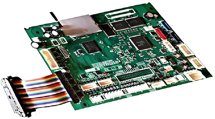
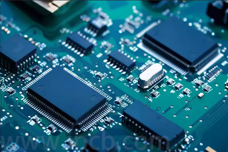
The camera motherboard, also called the camera pcb board, is one of the core components inside the camera and contains the camera’s processor. Memory. Interface chip. Sensor control chip and other important components. The role of the camera motherboard is to control and manage the various functions and operations of the camera, so that the camera can work properly.
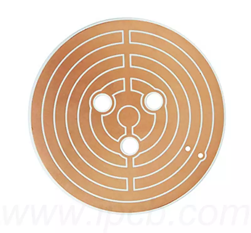
Camera pcb board composition structure
Camera pcb board as the core electronic components, the composition of its complex and multi-functional, mainly divided into the control module. Sensing module. Sensor module, storage module and application module. These modules work together to ensure that the camera can efficiently capture. Processing. Storage and display of images.
Control Module
The control module of the camera pcb board consists of a central processing unit (CPU). Digital Signal Processor (DSP) chip. Modem (MODEM) and wireless circuit and other key components.
Central Processing Unit (CPU): The CPU is the core processing unit of the camera, responsible for coordinating the operation of all modules and data processing.
Digital Signal Processor (DSP) Chip: The DSP chip, especially for cameras with CCD sensors, is mainly used to process and encode digital signals such as images. Sound and other digital signals. It may contain JPEG encoders, ISPs (Image Signal Processors) and USB device controllers.
Modem (MODEM): This component is used to implement communication with external devices to support wireless functionality.
Radio circuit: As the core component that enables wireless data transmission, it enables the camera to communicate wirelessly.
Sensing Module
The sensing module of the camera mainly includes CMOS or CCD image sensor. Flash control chip. Autofocus module. Optical filters and optical stabilisers etc.
CMOS or CCD Image Sensor: This is one of the core components of the camera and is used to convert optical signals into digital signals. A charge-coupled device (CCD) is an image detector based on a combination of passive photodiodes with high quantum efficiency and high pixel uniformity, but with a low frame rate. Complementary Metal Oxide Semiconductor (CMOS) detectors are based on a combination of active pixels and can achieve higher frame rates, but can suffer from higher noise and image inhomogeneity.
Flash control chip: This chip is used to control the flash on and off to ensure the right amount of light is available for the shot.
Autofocus module: This module enables focusing by adjusting the position of the lens to ensure image sharpness.
Optical filters: such as infrared cut-off filters, which are used to optimise the quality of light and thus improve the quality of the output image.
Optical stabiliser: responsible for providing image stability and reducing blur caused by camera shake.
Memory Module
The memory module of the camera pcb board consists of a cache, a memory chip and a memory card. The memory module is composed of a memory chip and a memory card.
Cache: As a temporary buffer for data processing and transmission, the cache can significantly speed up data processing.
Memory chip: Used to store data captured by the camera, such as photos and videos.
Memory card: External memory card is the main medium used to store photos. Video and other files.
Application Module
The application module of a camera pcb board usually includes the display. Buttons. Microphone. Speaker, USB port, etc.
Display: Used for real-time display of shooting results and camera settings information.
Buttons: Provide a user interface to control shooting and other functions.
Microphone and Speaker: The microphone is used to record sound and the speaker is used to play back sound.
USB Port: Used to connect to a computer for file transfer, printing and other data exchange functions. Printing and other data exchange functions.
The role of the camera pcb board
- Operation control: the camera motherboard through the processor to control the camera internal components of the communication and operation, to ensure that the camera can work properly.
- Image Processing: The processor and sensor controller on the camera’s main board can be obtained from the camera sensor for the original image noise reduction. Auto Focus. Colour balance. Post-processing and other operations to improve the camera shooting results.
- Storage Management: The storage management chip on the camera’s main board can control the camera’s internal memory to store and read photos and video files.
- Data transmission: the interface chip on the camera’s main board can control the camera and computer. Data transmission: the interface chip on the camera’s main board can control the camera’s data transmission with computers, mobile phones and other external devices. Communication and interconnection, to achieve the transmission and sharing of photos and video files.
- Power management: the power consumption controller on the camera pcb board can effectively control the power supply of the camera’s internal components to extend the battery life of the camera and improve the efficiency of the camera.
The working principle of a camera pcb board can be simply divided into the following steps:
- Conversion of optical signals into electrical signals: Camera circuit boards usually contain a photosensitive sensor, such as CMOS or CCD chips. When light hits the sensor, the photosensitive element converts the light signal into an electrical signal. This process involves the photoelectric effect, in which the energy of photons is converted into the energy of electrons.
- Electrical Signal Amplification and Filtering:The electrical signal output from the sensor is usually very weak and needs to be processed by amplification and filtering to improve the strength and quality of the signal. The amplifier circuit will increase the amplitude of the signal, while the filter circuit will remove noise and interference, making the signal more stable and clearer.
- Signal Processing and Coding:After the previous steps, the camera board has obtained a series of electrical signals representing the brightness values of each pixel point of the image. In the signal processing stage, these electrical signals will undergo a series of algorithms and processing, such as white balance. Exposure control . Contrast adjustment etc. to optimise the quality and detail of the image.
- Digital Signal Conversion and Compression:After signal processing, the electrical signals will be converted to digital signals for storage and transmission. This usually involves the use of analogue-to-digital converters (ADCs) to convert continuous analogue signals into discrete digital signals. The digital signal is also usually compressed to reduce the amount of data in order to reduce the cost of storing and transmitting the image data.
- Data transmission and display: after the digital signal conversion and compression, the image data can be transmitted in various ways, such as USB, HDMI, network and so on. Camera circuit boards usually also contain some interface circuitry in order to transmit the image data to the display device for display. The display device can be a TV. Computer monitors. Mobile devices etc.
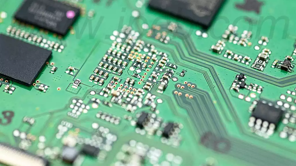
Types of Surface Finishes Suitable for Camera PCB board
Common surface finishing techniques for camera PCB board today include.
Hot Air Solder Levelling (HASL): This is a process whereby the PCB is flattened by immersing it in molten solder and then blown flat with a hot air knife to form a uniform coating. It provides good solderability and prevents copper oxidation.
Leaded Tin: Tin alloy containing lead.
Lead Free: An environmentally friendly process with less than 0.5% lead content, higher melting point and stronger solder joints.
Organic Solderability Protectant (OSP): Also known as organic solder mask or copper protectant, it is a process that chemically forms an organic protective film on the surface of bare copper. This film is resistant to oxidation, thermal shock and humidity, and is easily removed by the flux during soldering.
Electroless Nickel Immersion Gold (ENIG): This process forms a layer of nickel-gold alloy on the copper surface, which protects the PCB for a long period of time and is not easy to oxidise, making it suitable for long term storage. It is particularly suitable for the need for fine-pitch pins and small components soldering occasions.
Immersion Silver (Immersion Silver): Immersion Silver process in the PCB copper surface chemical deposition of a layer of silver, with good flatness and contact, suitable for communications products, automotive, computer peripherals and high-speed signal design.
Immersion Tin (Immersion Tin): chemically deposited on the copper surface of the tin metal plating, especially for communications backplanes, in the soldering place does not introduce new elements.
Electroless Nickel Electroless Palladium Immersion Gold (ENEPIG): This process is more commonly used in the semiconductor industry and has been gradually applied to PCBs in recent years. It is suitable for gold and aluminium wire bonding and has no nickel corrosion (black plate) problem and lower cost compared to ENIG.
Hard Gold Plating: Forms a layer of nickel-gold on the metal surface through an electrochemical reaction, especially suitable for contact connection designs such as gold fingers.
Electroplated Nickel-Gold: A layer of nickel is plated on the PCB surface followed by a layer of gold. The nickel layer is mainly used to prevent diffusion between gold and copper.
Key Attributes of PCB Finish Selection for Cameras
Selecting the right finish for a PCB design requires a combination of the following factors.
RoHS Compliance: Lead-free solder processes that comply with the RoHS (Restriction of Hazardous Substances) Directive should be preferred to meet environmental standards.
Handling sensitivity: Consider how sensitive the finish is to breakage or contamination during production and assembly.
Solderability: The finish should form a desirable solder connection to ensure a reliable component connection. For example, OSP and ENEPIG perform well in terms of solderability.
Compatibility with close-pitch components: Finishes should be suitable for close-pitch components such as BGAs (ball grid arrays) to ensure the quality of high-density assemblies.
Contactability: For areas where good electrical contact is required, such as keying areas or connectors, the finish should provide reliable contact performance.
Shelf Life: Finishes should have a long shelf life, preferably allowing storage for 6 months or more.
Additional Costs: The cost of different surface treatments varies greatly, which directly affects the overall manufacturing cost of the camera PCB board.
Camera PCB board is more than just a simple circuit board, they are the result of modern imaging technology and precision manufacturing. It is the result of modern imaging technology and precision manufacturing. Its sophisticated internal structure, efficient workflow, and diverse surface treatment technologies all contribute to the powerful functionality and excellent performance of the digital cameras we hold in our hands.