RF Filter PCB is circuit board specifically designed to process RF signals and are widely used in wireless communications, broadcasting, satellite, and other high-frequency applications. The main function of these circuit boards is to selectively allow certain frequency signals to pass through while suppressing or reflecting other unwanted frequency signals to improve system performance and stability.
The primary function of RF filters is frequency selectivity, which can be implemented in various types of filters such as band pass, band reject, low pass and high pass filters depending on the design needs. These filters are critical in many applications, especially at the receiver and transmitter front-ends of wireless communication equipment, to ensure clear transmission of the desired signal while reducing the effects of interfering signals.
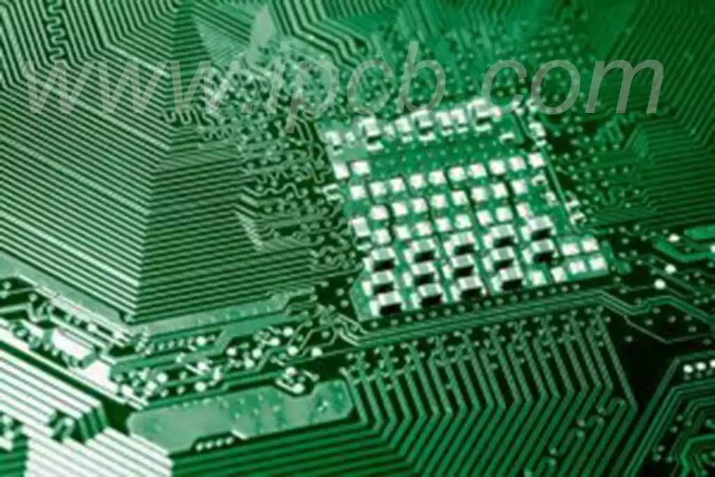
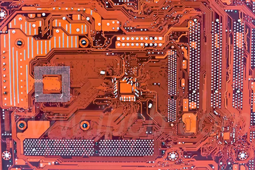
RF filters play a vital role in modern communication systems, and their PCB layout directly affects signal integrity and overall system performance. Therefore, when designing the PCB of an RF filter, special attention needs to be paid to layout specifications and techniques to achieve optimal performance.
1.Layout Planning
When laying out an RF PCB,you should first ensure that the components of the loop filter are arranged on the same layer and that the layout is as compact as possible. This arrangement helps to reduce signal transmission delay and distortion, while reducing the impact of noise. In addition, the relevant pins of the filter should be close together to facilitate signal transmission and stability.
2.Separation of power and control signals
The power and control voltage signals of the filter must be effectively isolated from other interfering signals. In the layout design,make sure that the power line of the filter is far away from high-speed signals and other lines that may cause interference, so as to reduce the adverse effects caused by signal aliasing and noise coupling.
3.Alignment design
RF signal alignment design should follow specific rules, such as the use of 45 ° angle of the turn to reduce signal reflection and loss. Ensure that the width and spacing of the output alignment meets the impedance matching requirements, which can significantly improve the performance of the filter and signal quality.
4.Ground Design
Ground level design is critical in PCB layout.Ensure that the high power area has a whole piece of ground, it is best to avoid the use of vias on the area, which can improve signal grounding and heat dissipation performance. At the same time, the increase in ground area can effectively enhance the stability of the filter and reduce the mutual interference between the signals .
5.Testing and Verification
After completing the rf filter PCB design, electrical testing is a critical step to ensure an optimized design. Through the use of network analyzers and other test equipment to detect the frequency response of the filter and other performance parameters, so as to verify the effectiveness of the layout design and make the necessary adjustments and optimization.
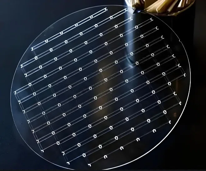
Material Requirements for RF Filter PCB
Substrate materials often used for RF filter PCB include FR4, polyimide and Rogers. Each of these materials has a different dielectric constant and loss angle tangent, and are suitable for a variety of high frequency and microwave applications.In RF, microwave and millimeter wave applications, Rogers materials offer stable dielectric constants and low loss properties for high performance applications.The dielectric constant (DK value) has a significant effect on the propagation speed and behavior of RF signals.When designing RF filters, a suitable dielectric constant needs to be selected to ensure good signal transfer and minimize reflection loss.
Different materials such as FR4 have a dielectric constant of around 4.0, while Rogers materials can have a dielectric constant as low as 2.2, which means that Rogers materials perform better in terms of signal integrity.
Thermal performance is also an important factor to consider when selecting a material. RF circuits generate heat during operation, so the material selected must be able to cope with high-temperature environments without performance degradation. In addition, proper thermal management design, such as the use of aluminum substrates, can also help improve device reliability.
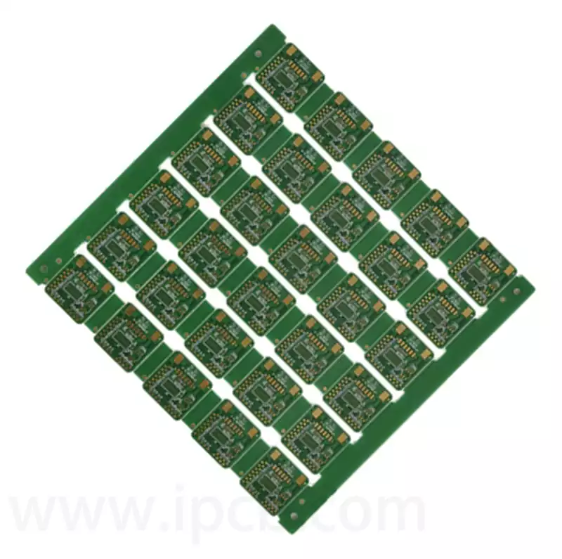
The quality and characteristics of the laminate materials are critical in the fabrication of RF filter PCBs. Semi-cured sheets (prepreg) should be selected based on their insulating properties and mechanical strength to ensure solid bonding and electrical performance between board layers. Also, the design of multilayer PCBs requires reasonable layer stacking to optimize signal integrity and EMC.
Key factors to consider when selecting a suitable RF filter PCB:
- Material Selection
The right PCB material has a significant impact on the performance of RF filters. Common RF PCB materials include FR-4, PTFE, RO3003, etc., with different dielectric constants and loss factors. Selection needs to be based on specific application requirements, taking into account the thermal characteristics and frequency response of the material to optimize performance. - Impedance Matching
Ensuring good impedance matching between the input and output ports of the filter is critical. Typically RF circuits are designed with a characteristic impedance of 50Ω to minimize signal reflection and loss. Impedance matching can be achieved by using matching circuits, transformers and Stubs during the design process. - Filter type
It is critical to select the proper type of filter based on the application requirements. Common filter types include low-pass, high-pass, band-pass, and band-stop filters. Choosing the right type of filter ensures effective signal transmission in the target frequency band and suppresses unwanted frequencies. - Electromagnetic Simulation Analysis
Electromagnetic simulation is an important tool when selecting a PCB. EM simulation software can predict the performance of the filter, including response, loss and group delay and other parameters. Special attention should be paid to high-frequency effects, such as signal propagation, reflection, and refraction, to ensure that the design is reasonable. - Cost and Size
Cost and size are factors that should not be ignored when designing filters. For mass-produced products, the material cost of the PCB and the manufacturing process need to be considered. In terms of size, the miniaturization trend is becoming more and more significant, and designers need to ensure that good performance is maintained in small sizes.
The main application areas of RF Filter PCB
1.Wireless communication
Wireless communication is one of the most important application areas of RF filter PCBs.They are widely used in cell phones, base stations, satellite communication equipment and other communication systems to ensure stable signal transmission and high quality reception. RF filter PCB can effectively screen out the effective signals and suppress the interfering signals so as to improve the communication quality.
2.Radar and remote control system
RF filter PCB in the radar system and remote control equipment also plays an important role. In radar technology, filters are used for signal selection and noise suppression to improve the clarity and accuracy of target detection.In remote control systems, these filters ensure clear transmission of command signals and reduce interference with other signals.
3.Medical Equipment
RF filter PCBs are becoming increasingly common in medical equipment, especially in medical imaging and monitoring equipment.They are used to filter out noise and unwanted signals, thus ensuring the accuracy and reliability of the equipment.For example, ultrasound and MRI equipment rely on high performance RF filters to ensure image quality and signal accuracy.
4.Consumer Electronics RF filter PCB is also widely used in consumer electronics, such as TVs, stereos, and smart home devices. They can improve the performance and reliability of the devices, and enhance the quality of audio and video signals by effectively filtering out unwanted high-frequency noise.For example, in audio amplifiers, filters ensure clear sound quality without noise interference.
5.Internet of Things (IoT)
With the rapid development of IoT technology, RF filter PCB is becoming an important part of IoT devices.In smart sensors and connected devices,RF filters can improve the anti-interference ability of the signal and ensure stable data transmission.
RF filter PCB plays a vital role in many fields such as modern communications, radar, medical equipment and consumer electronics.Reasonable design and effective layout can significantly improve the quality of the signal and transmission stability,so as to meet the strict requirements of high-frequency applications on the performance.The design process needs to fully consider the material selection,impedance matching and electromagnetic simulation and other factors to achieve the best performance.