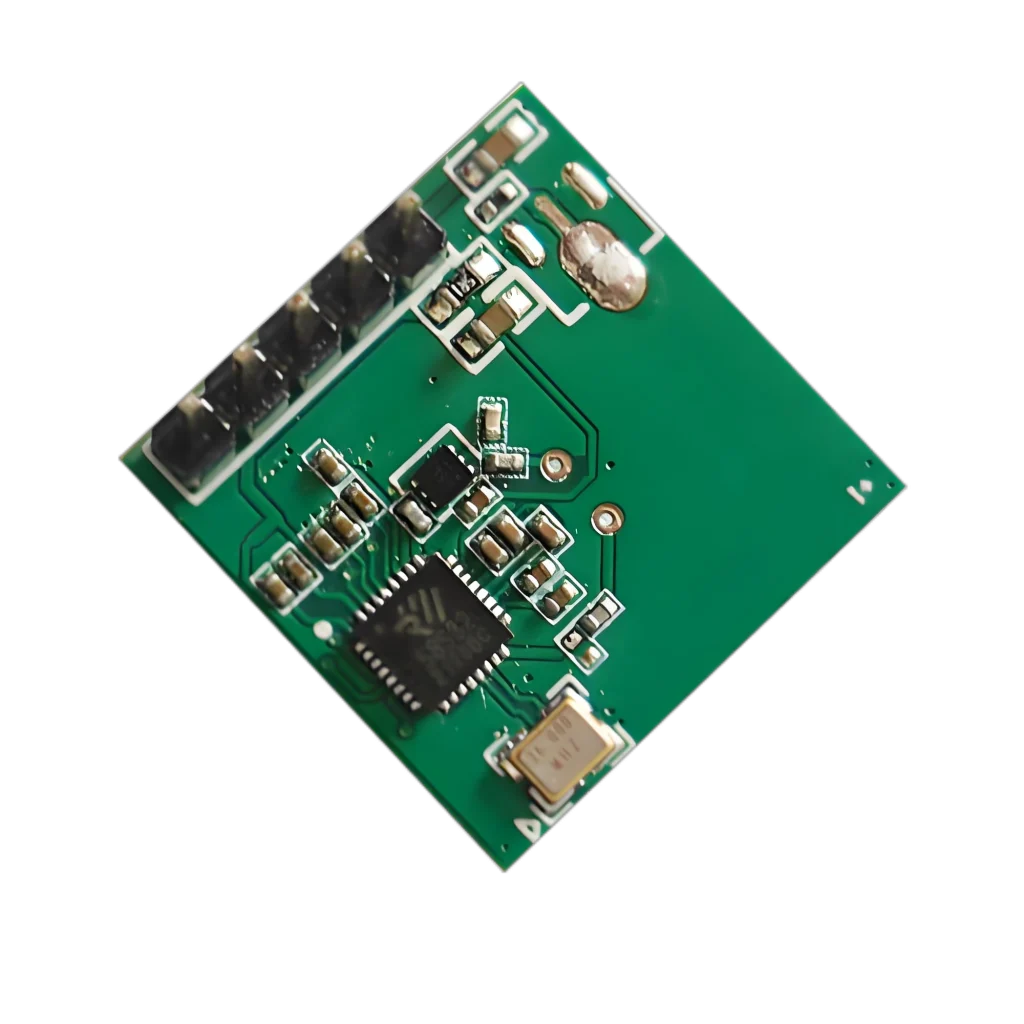
An IoT node often appears simple from the outside: a sensor collects data, a processor makes a decision, and a wireless link sends the result to the network. Inside the product, however, these functions are compressed into a module that may be only a few centimetres long. The same small board must accommodate radio-frequency transmission, digital processing, power conversion, sensing interfaces and, in many cases, local memory or security devices.This makes IoT module PCB assembly fundamentally different from assembling a conventional low-density control board.
Miniaturisation does not merely reduce the available placement area. It shortens electrical distances, increases thermal interaction between components, narrows the process window for soldering and makes many critical joints impossible to inspect visually.
Reliable manufacturing therefore depends on controlling the entire relationship between PCB design, solder paste deposition, component placement, reflow behaviour and post-assembly testing. In a compact IoT module, a small deviation in any one of these stages can influence RF performance, standby current or long-term field reliability.
Why an IoT Module Is Electrically Dense
An IoT module usually combines several circuit domains that behave very differently. The RF section contains an antenna, impedance-matching components, a transceiver and controlled signal paths. The digital section contains the MCU, memory, oscillators and communication interfaces. The power section may include a switching regulator, low-dropout regulators, battery monitoring and protection circuits.
These functions cannot simply be placed wherever empty board space remains. Fast digital edges can couple into the RF receiver. Switching-current loops can introduce noise into analogue sensors or the reference ground. Copper and components placed inside the antenna keep-out region can detune the antenna and reduce radiation efficiency.
The board must consequently be divided by function while remaining physically compact. RF traces should be short and referenced to a continuous ground structure. The antenna area needs controlled clearance from copper, components and mechanical structures. High-current switching paths must be compact, while sensitive analogue and RF circuits need separation from noisy power nodes.
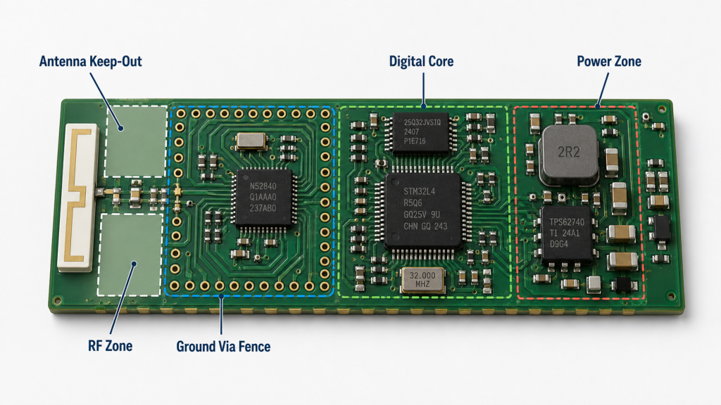
Ground-via fences are frequently used around RF regions to connect ground structures across PCB layers and reduce unwanted field propagation. Their effectiveness depends on via position, spacing and the continuity of the reference copper. Adding many vias without understanding the return-current path does not automatically improve shielding.
Design for Manufacturing Begins Before SMT
The manufacturability of an IoT module is largely determined before the first component reaches the placement machine. A dense layout can be electrically correct and still create unstable production if land patterns, solder mask clearances or component spacing leave insufficient manufacturing margin.
Fine-pitch QFN and LGA packages are common because they provide high functionality without exposed leads extending beyond the package body. Their hidden joints save space, but they also make solder paste design and thermal balance critical. The centre exposed pad often provides both electrical grounding and heat transfer. Excessive paste on this pad can lift the package and reduce the contact of perimeter terminals. Insufficient paste can weaken the thermal path or create discontinuous grounding.
Stencil apertures for large exposed pads are therefore normally divided into multiple smaller openings rather than printed as one continuous area. This controls solder volume, allows flux gases to escape and reduces package float during reflow. The aperture pattern must be matched to package geometry, via arrangement and required thermal performance rather than copied from a generic footprint.
Component spacing also has a direct manufacturing effect. If 0201 passives are placed too close to a tall shield frame, connector or inductor, the solder paste inspection and placement camera may have reduced visibility. Rework access becomes difficult, and local thermal mass can create uneven reflow behaviour.
The objective is not to make every clearance as small as the assembly line can theoretically achieve. It is to retain enough process margin for solder paste registration, component tolerance, placement deviation and production variation.
The Core Challenge: Depositing and Reflowing Very Small Solder Volumes
The most demanding stage of IoT module PCB assembly is often not component placement itself but the control of solder volume before and during reflow.
For 0201 components and fine-pitch ICs, each solder paste deposit contains a very small quantity of alloy powder and flux. Minor changes in stencil cleanliness, paste viscosity or board support can produce a significant percentage change in deposited volume. A deposit that appears only slightly misaligned may bridge adjacent pads or leave one termination with insufficient solder.
Stable printing begins with rigid board support. Thin or locally weakened panels can deflect under squeegee pressure, causing inconsistent contact between the stencil and PCB. Proper support tooling keeps the board surface flat during printing and reduces volume variation across the panel.
Stencil thickness must balance conflicting requirements. Small apertures need reliable paste release, favouring a thinner stencil, while power components and large thermal pads may require more solder. Step stencils or carefully modified aperture geometries may be used when one uniform thickness cannot satisfy both conditions.
Solder paste inspection is especially valuable at this stage because it measures the process before defects become hidden beneath components. Paste volume, height, area and positional offset can be monitored against statistical limits. The purpose is not only to reject an obviously defective print. Trend data can reveal gradual stencil blockage, paste degradation or alignment drift before the process produces widespread failures.
Placement accuracy is the next constraint. Very small components have little self-alignment margin, and their low mass makes them vulnerable to movement. Incorrect pickup height, nozzle wear or excessive placement pressure can deform the paste deposit or rotate the component. Package warpage and pad contamination further reduce the available process window.
Reflow then converts dozens or hundreds of independent paste deposits into permanent electrical joints. The thermal profile must activate the flux, evaporate volatiles, melt the alloy and cool the assembly without exposing components or the laminate to unnecessary thermal stress.
Compact IoT modules often contain both low-mass passives and thermally heavy structures such as shield frames, inductors or exposed-pad packages. These components do not heat at the same rate. If the profile is set only for the smallest components, large thermal masses may not remain above liquidus long enough. If it is made excessively aggressive, small components and laminate materials receive unnecessary heat exposure.
The profile must therefore be verified on the real product, with thermocouples positioned at representative hot and cold locations. Conveyor speed and oven-zone temperatures should be based on measured board behaviour rather than a generic recipe.
One of the characteristic risks for miniature passives is tombstoning. If solder melts or wets one termination earlier than the other, unbalanced surface tension can rotate the component into a vertical position. Unequal pad geometry, uneven paste volume, thermal asymmetry and excessive spacing between terminations can all contribute.
QFN and LGA packages create a different problem because their most important joints are hidden. Solder bridging, insufficient wetting and voiding beneath the exposed pad may remain invisible after assembly. This is why controlling the upstream process is more valuable than relying solely on final visual inspection.
Cleaning, Shielding and Mechanical Integration
After reflow, flux residues must be evaluated according to the solder paste chemistry and product environment. A no-clean process does not mean that every residue is harmless under every condition. Dense, low-voltage circuits may be sensitive to ionic contamination when exposed to humidity, especially around closely spaced conductors and high-impedance sensor inputs.
RF shield cans introduce another manufacturing interaction. The shield frame must be coplanar and fully soldered to the ground structure, but its thermal mass can change the local reflow profile. If the shield cover is installed before inspection or programming is complete, it may also conceal defects and reduce test access.
For modules assembled into a larger carrier board, castellated edge pads provide compact electrical connections. Their plating, routing quality and solder fillet formation affect both electrical continuity and mechanical strength. Dimensional variation at the board edge can influence how evenly the module sits on the carrier pads during secondary assembly.
Inspection Must Follow the Defect Mechanism
No single inspection method can confirm the quality of a compact IoT module PCBA. Automatic optical inspection is effective for visible defects such as missing components, polarity errors, displacement and abnormal solder fillets. It cannot directly evaluate solder joints hidden beneath bottom-terminated packages.
X-ray inspection provides visibility beneath QFN, LGA and similar packages. It can reveal solder bridges, insufficient coverage, displaced packages and abnormal void distribution beneath exposed pads. Interpretation still requires appropriate acceptance criteria: a visible void is not automatically a failure, but its total area, location and effect on thermal or electrical performance must be understood.
Functional testing then evaluates behaviours that structural inspection cannot confirm. A module may have visually acceptable solder joints yet draw excessive standby current, fail to start its oscillator or deliver weak RF output because of a damaged component, incorrect value or marginal connection.
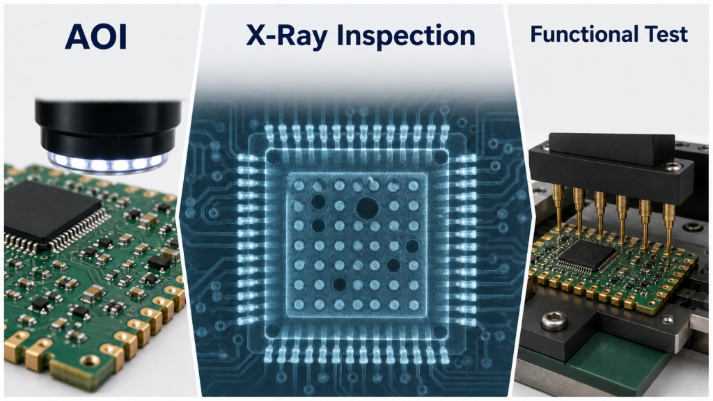
A useful functional test normally verifies power-rail behaviour, current consumption, firmware startup, communication interfaces and radio operation. RF testing should be designed around the product requirement. A basic connection test may be sufficient for some consumer nodes, while calibrated transmit power, receiver sensitivity or frequency-error measurements may be necessary for a qualified wireless module.
Test-point access should be designed into the PCB from the beginning. Retrofitting probe access after the layout is complete often introduces long stubs, weak mechanical contact or inaccessible pads. On very small modules, a combination of castellated-edge contacts, temporary programming pads and compact bed-of-nails fixtures may be used.
From Prototype Success to Stable Production
A prototype batch can appear successful even when the process has little production margin. Manual inspection, selective rework and slower placement settings can conceal weaknesses that become visible only when volume increases.
Before mass production, the manufacturer should review solder paste data, placement yield, reflow profile measurements, AOI findings, X-ray results and functional-test failures as one connected process. Repeated defects should be traced back to their mechanism rather than treated as isolated rework events.
For example, recurring voiding beneath one package may indicate an unsuitable exposed-pad aperture pattern rather than a reflow-only problem. Intermittent RF failures may originate from component placement near the antenna, inconsistent shield grounding or contamination around the matching network. Excessive standby current may be associated with leakage, an incorrect component value or partial solder bridging that remains within the limits of visual inspection.
Stable production is achieved when the process continues to produce acceptable modules despite normal variation in materials, machines and environment. The objective is not simply to manufacture one perfect sample, but to create a process window wide enough for repeatable output.
Engineering a Small Module as a Complete System
An IoT module PCB assembly compresses RF, digital, power and sensing functions into a small physical structure. Its manufacturing difficulty comes from the interaction between these domains rather than from component count alone.
Reliable production requires functional zoning, manufacturable land patterns, controlled solder paste deposition, accurate placement, a verified thermal profile and inspection methods matched to hidden defect risks. Electrical and RF testing must then confirm that the assembled module performs as a system rather than merely passing a continuity check.
iPCB provides PCB manufacturing and PCBA services for compact IoT modules from prototype verification to volume production. By reviewing PCB structure, component layout, stencil design, assembly conditions and test access before production, potential manufacturing and reliability risks can be identified before they become recurring defects.
In a miniature IoT node, precision is not defined only by how closely components can be placed. It is defined by whether every solder joint, signal path, power rail and RF function remains repeatable across the complete production process.