The significance of high-frequency PCB materials in 77 GHz automotive radar applications. Within the high-frequency spectrum, although numerous novel PCB materials have been developed, not all are suitable for such elevated frequencies. At millimetre-wave frequencies, which PCB material characteristics prove most critical? Understanding these properties facilitates the simplification of millimetre-wave applications, particularly concerning the selection of PCB materials for 77 GHz automotive radar systems.
High frequencies hold unparalleled commercial value due to their wider available bandwidth. As mobile phones, WLAN, and other commercial applications increasingly occupy lower frequency bands, millimetre wave bands at 60, 77, and even 94 GHz can meet the growing bandwidth demands of emerging applications such as fifth-generation (5G) cellular systems and automotive radar. Understanding fundamental material properties at millimetre wave frequencies is pertinent not only for 77 GHz PCB materials applications but also for the increasing number of high-frequency applications above 28 GHz.
Considerations regarding the dielectric constant (Dk) of PCB materials for 77 GHz automotive radar and other millimetre wave circuit applications involve two aspects: the intrinsic Dk of the base substrate material itself, and the design-related Dk associated with the circuitry. For the intrinsic substrate Dk, factors such as its tolerance and dispersion may be considered. Dk tolerance is a material parameter determined by variables in the laminate manufacturing process, where tighter tolerances may be required for certain applications.
Based on experience with high-frequency millimetre-wave circuits, a dielectric constant (Dk) tolerance of ±0.050 is generally considered acceptable. Dk dispersion is an inherent material property describing how the Dk value varies with frequency. Dk dispersion is particularly critical for broadband applications requiring coverage across extensive frequency ranges, such as the 77 GHz band.
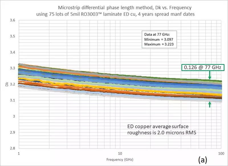
Design Dk represents the ‘working value’ of dielectric constant (Dk) determined for a specific circuit material formulation. Assessing its parameter variation proves challenging as design Dk is influenced by multiple factors. Furthermore, as pcb materials Dk increases, the propagation speed of electromagnetic waves within the circuit dielectric slows. Similarly, the copper roughness of printed circuit board materials affects the phase velocity of electromagnetic waves, thereby influencing performance at 77 GHz and other millimetre-wave frequencies (see Figure 1).
As shown in Figure 1, four distinct laminates and circuits were fabricated using the same 4mil LCP pcb materials. This LCP exhibits isotropic properties and delivers excellent performance across a broad microwave and millimetre-wave frequency range. While the dielectric properties of these four laminates are identical, they employ different copper foil types with varying surface roughness.
The term “different surface roughness” refers to the roughness of the copper foil surface at the interface where the copper foil meets the dielectric. This roughness was measured prior to the formation of the copper-clad laminate. Laminates with varying roughness were sent for PCB manufacturing to produce 50Ω microstrip transmission lines for testing. Each experimental group comprised two circuits that differed only in length, with all other parameters being identical.
Employing the microstrip differential phase length method, the effective Dk versus frequency relationship was determined by varying the circuit length. As illustrated in Figure 1, the circuit with the smoothest copper foil surface exhibited the lowest effective Dk. Conversely, circuits with rougher copper foils demonstrated an increasing trend in effective Dk. When solely considering differences in copper foil surface roughness, the variation in effective Dk across circuits was approximately 0.3.
For design purposes, circuits employing thinner materials are more susceptible to copper surface roughness than those using thicker substrates. For instance, if a thicker substrate were used in tests analogous to Figure 1, the difference in effective Dk values between varying copper surface roughnesses would be considerably smaller. As indicated by the four minor effective Dk curves in the figure, there is some variation with frequency. This variation relates to the dispersion characteristics of microstrip transmission lines and is also a consequence of material dispersion. When extracting Dk from effective Dk data, the Dk versus frequency curve (design Dk curve) typically exhibits a slight negative slope, as shown in Figures 2a and 2b.
和压延铜(b).webp)
The Dk versus frequency curves depicted in Figures 2a and 2b exhibit a normal trend, showing a slight negative slope as frequency increases. Even during Dk back-calculation, material dispersion will cause a slight decrease in Dk with frequency, in addition to the effects of microstrip line dispersion. The range of the design Dk value (~3.1) may appear substantial, but it is actually quite narrow, as numerous variables influence the design Dk.
For the pcb materials, the variation range of the dielectric constant Dk is only ±0.040 or ±0.080. Circuit fabrication also introduces some variation, such as changes in conductor width and trapezoidal effects. The trapezoidal effect refers to the shape of the signal conductor, which ideally has a rectangular cross-section but is often trapezoidal in actual circuits. Changes in conductor shape lead to variations in current density and edge field, and at higher millimetre-wave frequencies, these effects impact performance. The variation in the curve shown in Figure 2 is also related to substrate thickness tolerances, variations in the final copper plating thickness, and changes in the surface roughness of the copper foil.
Standard electrolytic (ED) copper used in circuits like those depicted in Figure 2a exhibits normal variations in surface roughness; typical values for ED copper in these circuits are 2.0 μm RMS, though actual roughness can range between 1.8 and 2.2 μm. Within this range of roughness variation, slightly smoother circuits exhibit lower design Dk values, while slightly rougher circuits yield higher design Dk values. For the design Dk range shown in Figure 2a (0.126 at 77 GHz), this represents a well-controlled design Dk tolerance (±0.063) considering the numerous variables influencing it.
Compared to Figure 2a, Figure 2b employs the same dielectric circuit material with smoother rolled copper, resulting in significantly reduced variation in design Dk. Although minor differences exist in circuit processing between electrolytic copper and rolled copper, this demonstrates that smoother rolled copper can minimise design Dk variation.
The surface roughness of copper foil and its variations exert a significant influence on the insertion loss of high-frequency microstrip circuits. Specifically, the rougher the copper foil surface, the higher the conductor loss, ultimately resulting in increased insertion loss. Furthermore, insertion loss is also related to the thickness of the circuit substrate. Thinner circuits are more susceptible to the effects of copper foil surface roughness, whereas thicker circuits are less significantly affected. For instance, on identical dielectric materials, the difference in insertion loss between thin circuits using smooth copper foil and those using rough copper foil is more pronounced than the difference observed between thick circuits employing the same copper foils.
At 25 GHz, when circuits employ 5 mil thick RO3003 material, the insertion loss difference between smooth rolled copper and rough ED copper reaches 0.35 dB/in. Using 20 mil thick RO3003 laminate for a similar comparison, the insertion loss difference between rough ED copper and smooth rolled copper circuits is 0.10 dB/in. These data clearly demonstrate that variations in copper foil surface roughness exert a more pronounced effect on insertion loss in thinner circuits, whereas millimetre-wave circuits typically necessitate relatively thin materials.
To demonstrate the impact of copper foil surface roughness, Figure 3 presents microstrip circuits on two similar PCB materials with identical (5mil) dielectric thickness but differing copper foil surface roughness. Both materials are widely employed in current 77 GHz applications, with Rogers’ RO3003 material having a long history and high shipment volume.
RO3003G2™ represents a newly introduced material, optimised specifically for 77 GHz automotive radar applications based on the RO3003 formulation. Given the similar Dk and Df values of both materials, the observed insertion loss differences are primarily attributable to copper foil surface roughness. The copper foil surface roughness for RO3003 material using standard ED copper typically measures 2.0μm RMS, whereas rolled copper yields a typical value of 0.35μm RMS. RO3003G2 employs ultra-low-profile (VLP) ED copper, achieving a surface roughness of just 0.7μm RMS.
Compared to ED copper foil on RO3003 laminate, RO3003G2 VLP ED copper foil significantly improves circuit insertion loss. Whilst still inferior to rolled copper in insertion loss performance, it offers substantial cost advantages over rolled copper. The material cost of VLP ED copper foil is slightly higher than that of ED copper foil, yet it delivers substantial savings compared to the more expensive rolled copper, alongside markedly improved insertion loss performance. Smoother copper foils, such as those akin to VLP ED copper foil, yield circuits with more consistent phase response. Conversely, for microvias employed in 77 GHz automotive radar circuits, smoother VLP ED copper facilitates laser drilling of microvias.
When selecting PCB materials for 77 GHz automotive radar, key considerations include dielectric constant (Dk) stability, copper foil surface roughness, thermal coefficient of dielectric constant (TCDk), moisture absorption, and glass fibre effects. These factors directly impact signal integrity, insertion loss, and system performance under harsh environmental conditions. With the advancement of millimetre-wave technology, new materials such as RO3003G2™ are being developed to enhance performance and control costs by optimising characteristics like copper foil roughness.
Future PCB materials development will continue targeting reduced loss, enhanced Dk stability, minimised Dk dispersion, and improved environmental adaptability. Thoroughly understanding and effectively managing these critical material properties is paramount for ensuring the reliability and high performance of 77GHz automotive radar systems, forming the cornerstone for driving continuous innovation in millimetre-wave technology.