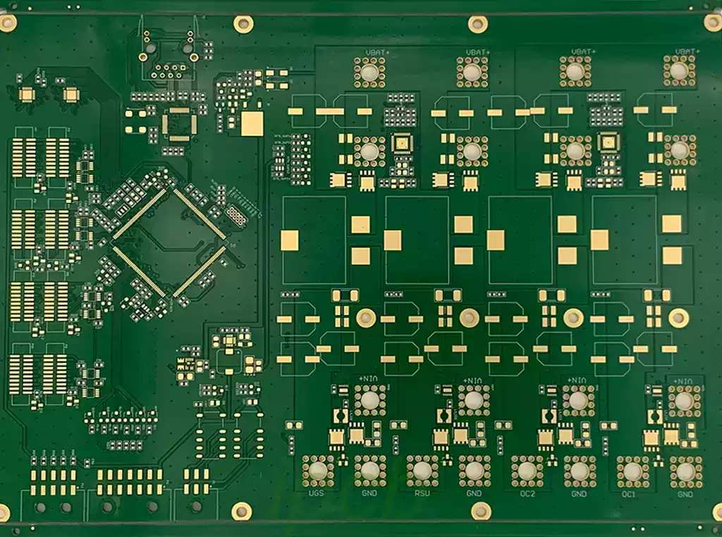
The PCB Bus Bar is one of the key components of a printed circuit board (PCB) and is primarily responsible for the transmission of current on the board. It is often presented as a flat metal bar with excellent conductivity and is widely used in electronic devices, circuit boards and electrical systems to transmit power, signals and data, and to carry out the distribution of electrical energy.
Bus bars play an important role in connecting, distributing and conducting current in circuits, and therefore play an important role in electronic equipment and electrical systems, and are becoming an integral part of the architecture of new energy vehicles.
Advantages of PCB Bus Bar:
Reduced power loop inductance
The PCB Bus Bar allows the current to flow closely inside the device, effectively reducing the loop area and hence the inductance. In high-speed and high-frequency applications where power supply stability is critical, it helps reduce voltage spikes and noise, significantly improving system stability.
Excellent current-carrying capability
Thanks to its high-quality conductive materials and large cross-sectional area, the PCB Bus Bar is able to efficiently transmit large currents, which is particularly suitable for power batteries, DC welders and other high-current-demanding application scenarios.
Enhanced Thermal Performance
The PCB Bus Bar efficiently conducts heat away from critical heat-generating components, reducing the need for additional cooling measures and improving overall thermal efficiency.
Space Optimisation
Its compact design not only reduces the use of multiple wire connectors, but also significantly saves space and reduces weight. This advantage is especially significant in industries such as aerospace and automotive, where equipment size and weight are critical.
Improved Reliability
PCB Bus Bars offer greater mechanical strength and durability than traditional wiring systems. Their rugged construction resists loose connections caused by vibration, resulting in higher reliability in harsh environments and demanding applications.
Simplified Assembly and Maintenance: By reducing the number of cables and connectors, the PCB Bus Bar simplifies the assembly process, speeds up installation and reduces the risk of assembly errors. It also facilitates troubleshooting and maintenance at a later stage.
Key factors to consider when designing a PCB Bus Bar:
Current Carrying and Thermal Management
The PCB Bus Bar must be able to effectively support the target current value without excessive heat build-up during full load operation.
Ease of processing and cost control
The design should be avoided to be too complicated, and the current transmission path should be planned in advance to minimise the number and length of lines passing through the PCB Bus Bar, in order to reduce the complexity and cost of production.
EMC Consideration
If the power supply or signal on the PCB bus bar is coupled with a high frequency signal, it may be transformed into an antenna effect, resulting in the external radiation of the device exceeding the standard. Therefore, EMC requirements need to be fully considered at the beginning of circuit design.
Details to focus on in the specific design of the PCB Bus Bar:
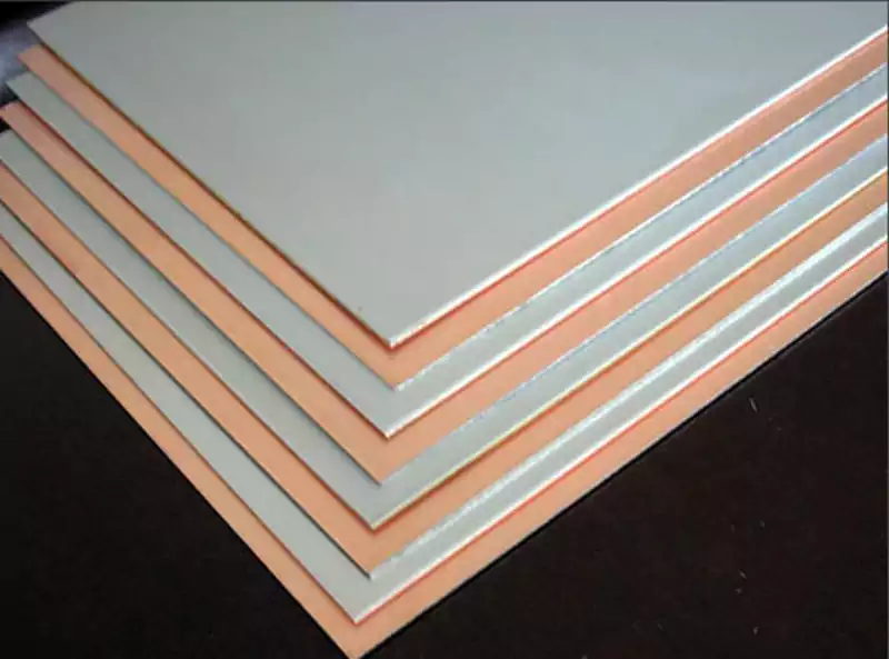
Copper foil thickness
The thicker the copper foil, the higher the current carrying capacity, but not the thicker the better. The thickness of the copper foil needs to be calculated accurately according to the designed voltage and current values.
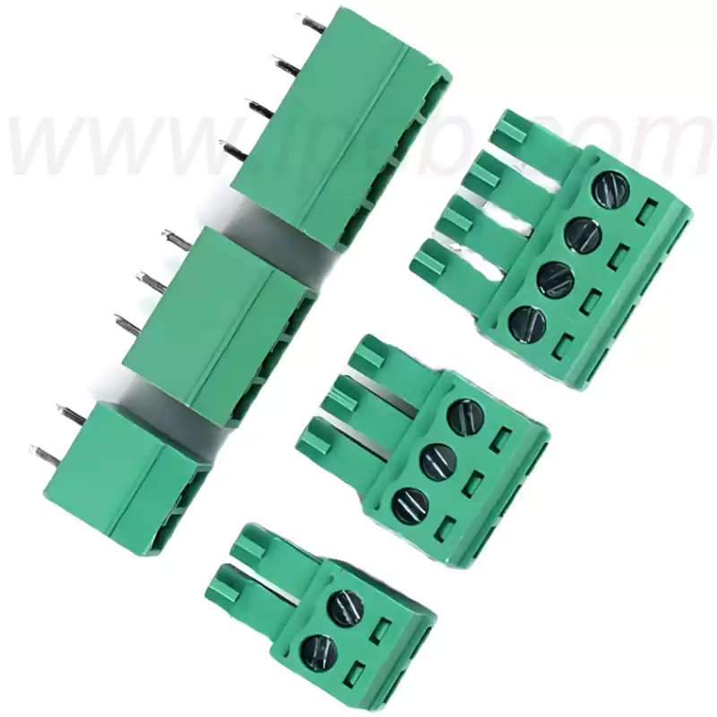
Current Carrying and Temperature Rise
PCB bus bars should be designed for a maximum current carrying capacity that is higher than the full load requirement, while keeping the temperature rise within a safe threshold. This is usually achieved by choosing the right conductor material and optimising its cross-sectional area, for example, for a current demand of 100A, a typical design would use a 5mm thick copper strip to ensure that the temperature rise does not exceed 20°C.
Resistance and Inductance Optimisation
Low resistance and inductance are at the heart of PCB bus bar design, and the shape, thickness and layout of the conductors all have an impact on this. For example, the use of trapezoidal or flat conductor forms can significantly reduce inductance and improve current transfer efficiency.
Electromagnetic Compatibility (EMC) Enhancement
PCB bus bars need to be designed in such a way that they do not cause excessive electromagnetic interference (EMI) and are resistant to external EMI. This can be achieved by optimising the conductor layout, applying shielding materials and other strategies to enhance the EMC of the PCB Bus Bar.
PCB Bus Bars play a vital role in electronic devices, as they are responsible for the efficient transmission and distribution of current and are an integral part of the printed circuit board. Their design advantages, such as reduced power loop inductance, increased current carrying capacity, optimised heat dissipation, space saving, enhanced reliability, and simplified assembly and maintenance processes, have led to the widespread use of PCB bus bars in a wide range of electronic devices, circuit boards and electrical systems.
During the design process, we need to take into account key factors such as current carrying and thermal management, processing convenience and cost control, and electromagnetic compatibility to ensure that the PCB Bus Bar meets the actual application requirements. At the same time, the choice of copper foil thickness, the balance between current carrying and temperature rise, the optimisation of resistance and inductance, and the enhancement of electromagnetic compatibility are also details that need to be given sufficient attention.
In the future, with the continuous development of electronic equipment, the application areas of PCB Bus Bar will be further expanded, and the requirements for its performance will also continue to improve. Therefore, we need to keep an eye on the latest progress of related technologies and optimise our designs to meet the market demand for high-performance and high-reliability PCB bus bars. Through continuous efforts and innovation, we believe that PCB Bus Bar will play a more important role in promoting the development of electronic equipment industry.
