Soldermask is a polymer coated on the surface of the copper foil of a PCB. Its main function is to cover the surface of the copper foil and prevent oxidation of the copper wires, thus extending the service life of the board. It also prevents the flow of solder between neighboring pads during soldering, which helps to ensure accurate and reliable soldering.
In Kicad, soldermask cleanup is usually done after the design is completed and before exporting the production file. The designer needs to carefully examine the board layout to identify any soldermask issues that may exist. This includes problems such as excess soldermask residue, too large or too small a gap between the soldermask and the pads, etc. Once the problem is identified, the designer needs to utilize the editing tools provided by Kicad to make precise cleanup and adjustments.
Kicad soldermask cleanup mainly involves the following aspects:
The removal of soldermask residues. These residues may be generated due to improper operation during the design process or defects in the software itself. With Kicad’s editing tools, designers can accurately identify and remove these residues, ensuring the integrity and accuracy of the soldermask.
Adjustment of the gap between the soldermask and the pads. If the gap is too large, it may lead to weak soldering; if the gap is too small, it may affect the precision and quality of soldering.Therefore,designers need to make precise adjustments to the gap according to the actual situation through Kicad’s editing functions.
Kicad also provides some automated tools to assist soldermask clearance. These tools can automatically detect and repair problems in the solder resist according to preset rules and parameters, greatly improving the efficiency and accuracy of the cleanup work.
In KiCad (and other EDAs), the soldermask layer is the “negative”. The graphic object on this layer means that the area will not be coated with “green oil” and the copper foil will be directly exposed to the air, i.e. the soldermask window.
There are three rules related to soldermask in the “Board Settings”:
Due to the terminology of different board manufacturers are slightly different as well as the problem of Chinese and English translation, the three soldermask settings in the figure above is not easy to understand, or easy to confuse, for example, many of my friends will feel that “soldermask expansion” (Solder mask expansion) and “soldermask to copper clearance” (Solder mask to copper clearance) seems to express the same meaning. Solder mask expansion” (Solder mask to copper clearance) seems to express a meaning. To understand the difference, you need to first understand the 3 scenarios that need to be considered in manufacturing:
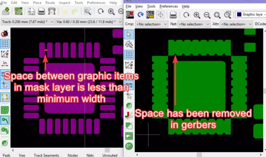
In the board setup, since it is a “negative”, the “Minimum Width of Soldermask Bridge” for a soldermask layer refers to the physical soldermask, not to the graphic objects in the layer. From the layer’s point of view, it means the minimum allowable gap between graphic objects. The soldermask minimum width is always global and is similar to the area minimum width, even though the soldermask layer is “negative”. This means that if the gap between two graphical objects in the F.Mask or B.Mask layer is smaller than the set minimum, these objects will be fused together when generating the Gerber.
Kicad soldermask clearance is an important task in circuit board design. By mastering the correct cleaning methods and techniques, designers can ensure the reliability and performance of the board, providing a strong guarantee for the successful manufacture of electronic products.