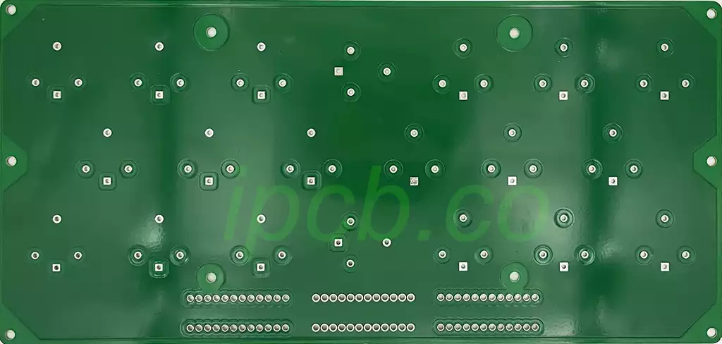
In the field of modern electronic hardware engineering and printed circuit board (PCB) design, two-layer PCBs continue to hold a crucial position in consumer electronics, industrial control, IoT terminals, home appliances, and automotive electronic auxiliary modules due to their high cost-effectiveness, mature manufacturing processes, and simplified supply chain management. However, compared to multilayer PCBs (such as four-layer, six-layer, and HDI boards) with independent power and ground layers, two-layer PCBs only have two usable conductive copper foil layers: the top layer and the bottom layer. Within such a limited physical space, constructing a low-impedance, continuous, and highly efficient ground plane has become the core technical bottleneck determining the overall electromagnetic compatibility (EMC), signal integrity (SI), and power integrity (PI) of the board.
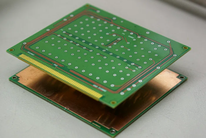
Many junior hardware engineers, when designing two-layer PCBs, often simply understand the ground plane as “filling the remaining blank areas with copper pour and connecting it to GND after the circuit board routing is completed.” This traditional understanding of ground as a static potential node is the main reason why many double-layer boards encounter excessive high-frequency noise, extremely poor electrostatic discharge (ESD) immunity, signal edge distortion, and large fluctuations in analog-to-digital converter (ADC) sampling during hardware testing.
In reality, in dynamic high-frequency circuits, the ground plane is not a static conductor, but rather a “dynamic return path” in the closed loop of all signal currents and power supply currents. A deep dive into the electrical nature of the 2 layer pcb ground plane, the microscopic current return mechanism, the logic of meshed copper pouring, the placement of stitched vias, mixed-signal segmentation strategies, and the physical engineering pitfall avoidance principles has irreplaceable technical value for building highly reliable hardware systems.
The Electrical Nature of the Double-Layer Board Ground Plane and its Triple Core System Functions
To understand the design principles of the ground plane, it is first necessary to redefine the ground plane at the electromagnetic level. In a direct current (DC) circuit, current flows along the path of least resistance; in this case, the ground wire only serves as a low-resistance conductor for current to return to the negative terminal of the power supply. However, even digital chips in modern electronic devices, with a main frequency of only tens of megahertz, often have signal rise/fall times reaching nanoseconds or even sub-nanosecond levels. This results in signals rich in high-frequency harmonic components reaching hundreds of megahertz. Within the realm of alternating current (AC) and high-frequency electromagnetic fields, current always flows along the closed path of “minimum impedance” (i.e., minimum inductive reactance).
In this physical context, the ground plane on a double-layer board performs three intertwined system functions:
Providing a high-frequency return path with the lowest impedance and smallest loop area.
According to Maxwell’s electromagnetic theory, any current must flow in a closed loop. When a signal line is transmitted on the top layer, there must be a mirror-induced current of equal magnitude but opposite direction on the reference plane (ground copper foil) directly below it. When the double-layer board has a continuous and complete ground plane, the high-frequency return current can flow close to the copper foil area directly below the signal trace, making the physical loop area formed by the signal path and the return approach zero. According to the electromagnetic radiation formula, the electromagnetic energy radiated outward by a circuit is proportional to the square of the loop area. Therefore, minimizing the return loop area is the most effective way to suppress electromagnetic interference (EMI) and improve immunity to external electromagnetic interference (EMS) at its source.
Suppressing Ground Bounce and Establishing a Unified Reference Potential: When multiple digital chip output pins simultaneously switch between high and low levels, a large current flows into the ground network instantaneously. According to the principle of electromagnetic induction, if parasitic inductance exists in the ground path, this transient large current will induce high-frequency voltage fluctuations in the ground path, the so-called “ground bounce” or switching noise. Ground bounce can cause logic chips to misinterpret high levels as low levels, or cause drastic drift in the reference point of sensitive analog circuits. A large-area, multi-point interconnected double-layer board ground plane can greatly reduce the overall parasitic inductance of the ground network, smooth transient voltage fluctuations, and provide a stable and unified zero-potential reference plane for the entire board.
Thermal Management and Board Mechanical Stress Balance: In addition to electrical functions, the double-layer board ground plane also plays a crucial physical role. Modern surface-mount devices (such as MOSFETs, high-power LEDs, three-terminal regulators, and microprocessors) generate concentrated heat during operation. Large-area ground plane copper foil possesses extremely high thermal conductivity, acting as a natural heat sink to rapidly conduct and evenly distribute heat from device leads and underlying thermal pads across the entire board surface, significantly reducing local junction temperature. Furthermore, during the high-temperature reflow soldering process on a PCB, if the copper foil coverage of the top and bottom layers is severely asymmetrical, uneven internal stress will occur due to the coefficients of thermal expansion, leading to severe physical warping or twisting of the final board. Laying a large-area ground plane on the bottom layer can balance the copper foil weight on both sides, ensuring the flatness of the physical structure.
Signal Return Flow Physical Mechanism and the Physical Catastrophe of Ground Slotting
In double-layer board designs, the most easily overlooked physical phenomenon is the disruption of the high-frequency return path caused by “ground slotting.”
In multilayer boards, a dedicated ground plane is typically uninterrupted by signal lines; however, in double-layer boards, due to limited space on the top layer, engineers are often forced to route some signal or power lines on the bottom layer. Every long trace passing through the bottom layer, or a row of densely packed through-hole pins (such as connector pins), creates a physical “cliff” or “slit” on the ground copper foil of the bottom layer.
Return Current Detours and Increased Loop Area: When a high-frequency signal line on the top layer crosses the slit on the bottom layer, its mirrored return current flows along the ground plane to the edge of the slit where it is interrupted. Since the high-frequency current cannot penetrate the insulating substrate (FR-4), it is forced to change its path, detouring along the physical opening at the edge of the slit until it reaches the end of the slit, bypasses it, and then returns to flow under the signal line.
This return current detour phenomenon has extremely adverse engineering consequences:
Antenna Effect and Increased Electromagnetic Radiation: The originally tightly coupled signal line and return line are forcibly separated at the slit, forming a huge slot antenna structure. This exposed large loop area strongly emits electromagnetic waves, causing the product to severely exceed conducted and radiated emissions (RE) limits during electromagnetic compatibility testing.
Signal waveform distortion: The bypass path significantly increases the parasitic inductance of the return path, causing a drastic change in the characteristic impedance of the signal transmission line at that point. This impedance discontinuity leads to severe overshoot, undershoot, ringing, and edge delay in high-frequency signals, directly reducing the timing margin of the digital system.
Return path overlap and electromagnetic crosstalk: When multiple parallel high-frequency signal lines simultaneously cross the same ground plane slit, their respective return currents are forced to bypass the slit edge, resulting in compression within the same narrow conductive area. This physical overlap of return currents leads to severe “common impedance coupling,” directly injecting high-frequency noise from one signal line into adjacent signal lines, generating transient crosstalk faults that are difficult to diagnose.
Topology Construction Strategies and Engineering Methodology for Ground Planes on Double-Layer Boards
Given the inherent limitation of the number of physical layers in double-layer boards, to construct a low-impedance, high-continuity ground plane, it is essential to abandon the erroneous practice of haphazardly laying copper after random routing and instead adopt a rigorous topology engineering strategy from the initial layout and routing stages.
Establishing the Primary Ground Plane Logic
When designing a double-layer board, the bottom layer must first be clearly designated as the “primary ground plane.”
In terms of routing priority, the top layer should handle over 80% of signal traces, power traces, and component placement. The bottom layer should be considered a “sacred and inviolable physical reference layer.” The bottom layer must retain a large, solid area of ground copper foil. Only in extremely special cases where intersections with the top layer are not possible should a very small number of short jumpers be allowed on the bottom layer. All short traces on the bottom layer must adhere to the principle of “as short as possible, strictly prohibiting long parallel traces,” and the routing direction should be kept as consistent as possible to prevent the bottom layer from being fragmented into isolated areas.
3D Grounded Grid System: On some high-density, highly complex double-layer boards, the bottom layer inevitably suffers from numerous signal lines breaking the circuit, making large-area continuous copper pours impossible. In such cases, a “grid-based grounding strategy” should be employed to salvage the system’s electromagnetic performance.
The core implementation rules of grid-based grounding are:
- On the top layer, all signal traces extend primarily along a specific axis (e.g., the vertical Y-axis);
- On the bottom layer, all bridging traces extend primarily along a vertical axis (e.g., the horizontal X-axis);
- After routing, fill all unused areas on both the top and bottom layers with grounding copper foil;
- At the intersections of the top and bottom layer ground copper and in dead zones, densely insert grounding vias.
Through this crisscrossing layout, although the copper foil appears cut on one side, in three-dimensional space, the vertical ground lines of the top layer and the horizontal ground lines of the bottom layer intertwine through numerous physical vias, forming an extremely dense three-dimensional “grid-based ground network.” This mesh network compresses any possible return current routing distance into extremely small mesh cells, thereby keeping high-frequency loop inductance within safe thresholds.
Shielded Ground Enclosure and Coplanar Waveguide Structure
For critical sensitive signals on double-layer boards (e.g., weak analog sensor input signals, high-gain amplifier feedback lines) or strong radiation sources (e.g., crystal oscillator clock lines, PWM drive lines of switching power supplies), relying solely on the lower ground plane is often insufficient.
In such cases, a “ground enclosure” treatment must be implemented within the same plane. Specifically, two parallel strip-shaped grounding traces are laid on both sides of the critical signal lines on the top layer, forming a coplanar “ground-signal-ground” structure. To prevent these ground enclosure traces from forming suspended antennas, a stitched via must be placed at regular physical intervals along the extension direction of the ground enclosure traces, directly connecting them to the main ground plane of the lower layer. This structure electromagnetically constitutes a coplanar microstrip line, greatly confining the electromagnetic field between the signal lines and the ground lines on both sides, significantly reducing outward radiation and inward electromagnetic coupling.
Physical Mechanism and Placement Physics of Stitching Vias
In double-layer copper plating design, GND (Ground-ND Stitching Vias) are the core components connecting the top and bottom ground planes, ensuring the three-dimensional electromagnetic continuity of the ground plane. Many designers use stitching vias arbitrarily, either placing too many, disrupting the physical rigidity of the substrate, or placing too few, leaving fatal electromagnetic loopholes.
The Triple Physical Functions of Stitching Vias:
- Eliminating Floating Copper/Dead Copper and Antenna Effects. After automatic copper plating in software, due to the obstruction of dense traces and component pins, some “dead copper” or “isolated copper foil” with only one end connected or no connection at all often appear at the edges of the board or in the gaps between traces. These floating conductors generate standing waves under electromagnetic field excitation, becoming highly destructive radiating antennas. By placing stitching vias, these isolated copper pieces can be forcibly anchored to the main ground potential of the bottom layer, transforming them into effective shielding.
- Reducing the Potential Difference and High-Frequency Impedance Between the Two Ground Planes. Due to phase delay and self-inductance effects when high-frequency current flows on the conductor surface, a slight transient potential difference exists between the top and bottom ground copper layers when they are not connected. A dense array of vias provides hundreds or thousands of parallel miniature low-inductance paths between the two layers. Based on the principle of parallel inductive superposition, this significantly reduces the high-frequency impedance of the overall ground network and eliminates cavity resonance between the two ground planes.
Creating a “Faraday Cage” shielding wall at the board edge. The edges of a PCB are often weak points for electromagnetic wave leakage and external electrostatic discharge (ESD) intrusion. A continuous array of stitched vias (the so-called “Via Fence”) arranged at regular intervals along the outer perimeter of the double-layer board encloses the top and bottom ground copper layers in a three-dimensional metallic enclosure, effectively preventing high-frequency noise from radiating from the board edge and preventing electrostatic discharge from damaging internal traces along the board edge.
The Physical Calculation Rules for Seam Via Spacing
The density of seam vias is not blindly higher; excessively dense drilling can compromise the mechanical bending strength of the PCB substrate and potentially disrupt copper traces in inner or bottom layers.
In electromagnetic engineering, the physical determination of via spacing depends on the wavelength of the highest effective operating frequency within the system.
For digital circuits, the highest effective frequency of a signal is not determined by the clock frequency, but rather by the signal’s rise time. Its cutoff frequency can be expressed as 0.35 divided by the signal rise time. To ensure that the shielding barrier formed by vias effectively reflects and cuts off high-frequency electromagnetic waves, the maximum physical spacing between seam vias (denoted by the letter D) must be much smaller than the wavelength of the high-frequency signal in the PCB medium (the dielectric constant of FR-4 substrate is typically between 4.2 and 4.8, denoted by the Greek letter Lambda).
The golden rule strictly followed in engineering practice is that the maximum spacing of stitched vias should be less than or equal to one-twentieth of the wavelength of the highest effective frequency, and in extremely demanding applications, it should be controlled within one-tenth:
Extremely high frequency and steep edge regions (e.g., above several hundred megahertz): The stitched via spacing should generally be strictly controlled within two to three millimeters.
General digital and low-frequency mixed signal regions: The stitched via spacing can be extended to four to six millimeters.
Via fence: The via spacing is recommended to be maintained between 1.5 and 2.5 millimeters to form a dense anti-static and electromagnetic shielding barrier.
Ground Plane Segmentation Engineering for Mixed-Signal and High-Voltage Isolation Areas
On double-layer boards containing analog and digital circuits (e.g., boards with high-precision sensor sampling and MCU control) or high-voltage and low-voltage control circuits, ground plane design involves extremely complex signal isolation and safety specifications. Blindly laying copper across the entire board or indiscriminately cutting ground planes can lead to disastrous engineering consequences.
The Correct Handling Strategy for Analog Ground (AGND) and Digital Ground (DGND)
In traditional hardware design concepts, many tutorials blindly emphasize physically separating “digital ground” and “analog ground,” bridging them at a single point with a ferrite bead or a zero-ohm resistor. However, on double-layer boards with only two conductive layers, this forced grounding practice is extremely dangerous most of the time.
If a ground plane is physically cut on a double-layer board, any digital or analog signal line that has to cross this cut will have its return current forced to detour significantly, resulting in severe electromagnetic radiation and noise backflow.
The optimal design paradigm for modern high-reliability mixed-signal dual-layer boards is physical partitioning, not ground plane splitting, adhering to a unified ground plane.
Specific engineering implementation steps are as follows:
Physical Partitioning of Component Layout: The PCB is clearly divided into “analog” and “digital” areas. All sensors, operational amplifiers, ADC chips, and reference sources are concentrated in the analog area; all MCUs, digital buses, clock crystals, and switching power supplies are concentrated in the digital area.
Maintaining Integrity at the Bottom Layer: The bottom layer remains a single, completely continuous, uncut low-impedance ground plane.
Natural Isolation of Current Paths: Based on the aforementioned physical return current mechanism, the return current of high-frequency signals in the digital area automatically flows directly beneath the top-layer digital traces and will never actively drift beneath the analog area; similarly, the return current of analog signals also flows directly beneath the analog traces. By employing a well-designed physical spatial layout and utilizing the “self-optimizing characteristic” of high-frequency return current, natural physical isolation between digital and analog currents can be achieved on the same continuous ground plane. This eliminates ground potential drift and avoids electromagnetic compatibility (EMC) failures caused by cross-slot return current.
High-voltage isolation zone safety distance and physical slotting: Unlike low-voltage mixed signals, in power supply double-layer boards involving 220V AC mains input and high-voltage DC drives (such as motor drivers and inverters), absolute physical separation and hard isolation must be implemented between the high-voltage ground (primary side ground) and the low-voltage safety ground (secondary side human-machine interface safety ground).
This isolation is not only an EMC requirement but also a mandatory requirement related to personal safety and safety certifications (such as IEC 62368 and UL 60950).
In such areas, ground plane design must meet clearance (shortest distance in air) and creepage distance (shortest distance along the surface of the insulating medium) specifications:
Complete disconnection between high and low voltage ground planes: A physical keepout zone of several millimeters or more must be maintained between the grounding copper foil in the high-voltage area and the grounding copper foil in the low-voltage area, prohibiting the presence of any conductive copper foil.
Milling physical isolation slots (Air Slots): To prevent high-voltage arcing breakdown along the FR-4 insulating substrate surface due to increased atmospheric humidity or surface dust, a CNC milling cutter must be used to directly hollow out the PCB substrate in the insulating area between the two grounds, forming an air isolation slot that penetrates the board. Since the dielectric breakdown strength of air is much higher than that of a contaminated substrate surface, physical milling can significantly improve high-voltage isolation protection capabilities.
Practical Engineering Pitfalls and Checklist for Double-Layer Board Ground Plane Design
During the hardware engineering production and mass production (NPI) stages, improper handling of many small layout details can render a meticulously designed ground plane ineffective. The following summarizes the most common engineering defects in double-layer board ground plane designs and corresponding solutions:
Thoroughly Eliminate “Long Thin Copper Fingers”
After automatic copper plating in software, extremely narrow, long strips of copper foil often get squeezed into the gaps between dense cabling or around chip pins. These “copper tongues” typically have only one end weakly connected to the main ground network, while the other end extends deep into the high-frequency signal area.
Engineering Hazards: Under the influence of electromagnetic fields, these long thin copper tongues have extremely high high-frequency parasitic inductance. They not only fail to provide a good ground reference but also form a highly efficient dipole radiating antenna, powerfully emitting board noise.
Solutions: During final design review, all long thin copper strips with a width less than a certain threshold (e.g., 0.5 mm) or severely disproportionate aspect ratios must be forcibly removed according to the EDA software’s inspection rules. If ground copper is indeed needed in this area, a via must be added at the end of the copper tongue to connect it to the underlying layer.
Minimizing Parasitic Inductance of the Decoupling Capacitor Ground Path
Decoupling capacitors, placed near chip power pins, primarily function to provide high-frequency current to the chip instantaneously and suppress high-frequency noise on the power lines. The effectiveness of a decoupling capacitor depends entirely on the parasitic inductance of its connection loop.
Engineering Error: Many engineers extend the ground terminal of a decoupling capacitor several millimeters or even centimeters through a thin trace before connecting it to a nearby ground via or ground copper foil.
Solution: The ground pin of a decoupling capacitor must be directly drilled into the main ground plane using the shortest possible trace, the widest possible wire diameter, and the most convenient via method. The optimal via method is “parallel vias next to the pads,” and it is strictly forbidden to use long traces to connect the ground terminals of multiple capacitors in series.
The Conflicting Balance Between Thermal Relief and High-Frequency Conductivity
When connecting copper plating to the ground pad of a surface mount component (SMT) or through-hole (PTH) pin, the software defaults to generating a “cross-shaped” thermal relief pad. This design uses four narrow copper branches to connect the pad to a large area of ground copper. Its purpose is to reduce heat dissipation during wave soldering or manual soldering, preventing the large copper foil from absorbing heat too quickly, which could lead to unmelted solder and tombstoning.
Engineering Contradiction: For high-frequency decoupling capacitors, RF matching components, and the base heatsink pads of high-power chips, the narrow copper branches introduced by the cross-shaped thermal relief pad introduce significant parasitic inductance, greatly weakening high-frequency filtering and heat dissipation performance.
Solution: For high-power heat dissipation pads and grounding pads for high-frequency decoupling capacitors, provided there is a good automated reflow soldering process, they should be decisively modified to “Full Connection/Direct Connect” mode; for ordinary low-frequency component pins, the cross-shaped thermal pads should be retained to balance soldering production yield.
Comprehensive Design Archiving Checklist: Before submitting the double-layer PCB file to the factory for board fabrication, the following ground plane-specific reviews must be performed item by item:
Has the bottom layer been clearly designated as the “primary reference ground plane,” and has the total length of the bottom layer traces been compressed to the limit?
Has the high-frequency signal traces on the top and bottom layers been thoroughly checked to ensure that there are no cuts across the bottom layer ground plane?
Has a complete perimeter of via fencing been arranged around the entire board edge at intervals within one-tenth of the wavelength?
Has all floating dead copper and thin floating copper tongues been removed from the entire board?
Have the analog and digital circuit areas been physically separated, and is a complete and unified ground copper layer maintained on the bottom layer?
Are all decoupling capacitor ground vias placed close to the pads, and are the connection traces short and thick?
Do the electrical clearances between the high-voltage and low-voltage isolation areas meet the standards, and have the necessary physical air isolation channels been drawn?
By deeply understanding the nature of the return current’s movement in the microscopic electromagnetic field, abandoning the traditional “static grounding” mindset, and consistently maintaining the physical continuity of the bottom ground plane in the layout and routing, even on double-layer PCBs with limited physical layers and extremely sensitive cost, hardware engineers can still design excellent hardware systems with superior electromagnetic compatibility, clean and stable signals, and industrial-grade high reliability.