During the operation of various electronic devices, components mounted on internal PCBs continuously generate heat due to electrical power consumption. Without scientifically optimized and efficient pcb thermal management solutions, the accumulated heat cannot be effectively transferred and dissipated, resulting in excessive internal temperatures and long-term thermal stress.
Under high-temperature operating conditions, the electrical performance and physical stability of electronic components gradually deteriorate, significantly increasing the risk of aging, damage, and functional failure. This directly affects the operational stability, service life, and overall reliability of electronic equipment. Therefore, integrating a comprehensive thermal management strategy during the PCB design stage is a critical factor in ensuring long-term and reliable operation of electronic systems.
Improving Thermal Performance Through PCB Substrate Optimization
The PCB substrate materials widely used in the electronics industry today mainly include epoxy glass-fiber laminates and phenolic resin glass-fiber laminates, while some low-cost applications still rely on paper-based copper-clad laminates. Although these conventional materials provide excellent electrical insulation, mechanical strength, and manufacturability, they generally suffer from low thermal conductivity and limited heat dissipation capability.
In traditional thermal management approaches, resin-based PCB substrates provide very limited heat conduction capability. As a result, heat generated by electronic components can only be released through natural convection from the component surface to the surrounding air. However, with the continuous development of electronic products toward miniaturization, higher integration density, and increased power consumption, PCB routing density and component integration levels have increased significantly. Natural convection alone is no longer sufficient for high-power applications.
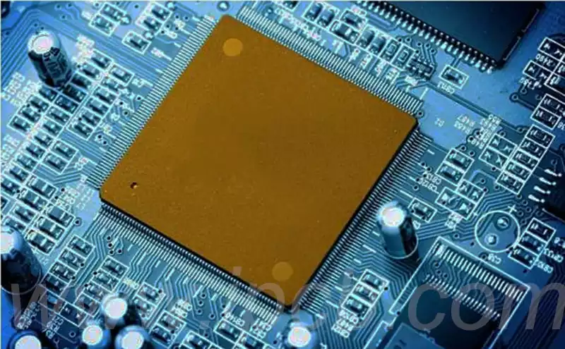
For surface-mounted components such as QFP and BGA packages, a large amount of heat is directly transferred into the PCB surface, creating severe localized thermal accumulation. Therefore, improving the intrinsic thermal performance of the PCB itself and enhancing the heat conduction and spreading capability of the board material have become fundamental approaches for solving thermal accumulation issues.
During the PCB layout design stage, component placement should be determined according to thermal conditions and heat distribution characteristics. Temperature sensing components should be accurately positioned in areas with the highest expected operating temperature to monitor peak temperatures in real time and provide reliable data for thermal protection and cooling control.
Meanwhile, temperature-sensitive components and devices with strict thermal limitations should be placed away from high-temperature regions and located in cooler areas with sufficient airflow. This prevents excessive heat exposure from affecting measurement accuracy, electrical characteristics, and operational stability.
Component zoning principles should also be followed by classifying devices according to their heat generation levels and thermal tolerance. Low-power components such as small-signal transistors, small-scale integrated circuits, and electrolytic capacitors generally generate less heat but have lower temperature resistance. These components should be placed in upstream airflow regions where cooling air enters the system, ensuring operation under relatively lower temperatures.
High-power components, including power transistors and large-scale integrated circuits, generate significant heat and typically have higher thermal resistance. These devices should be arranged in downstream airflow areas to prevent the heated airflow generated by high-temperature components from affecting thermally sensitive devices.
For high-power components, a three-dimensional thermal layout strategy should be implemented. In the horizontal direction, high-temperature devices should be positioned as close as possible to the PCB edge to shorten heat conduction paths and facilitate heat dissipation toward external structures.
In the vertical direction, these components should preferably be placed in upper areas of the PCB assembly to reduce thermal radiation impact on lower-positioned components and minimize secondary heating effects.
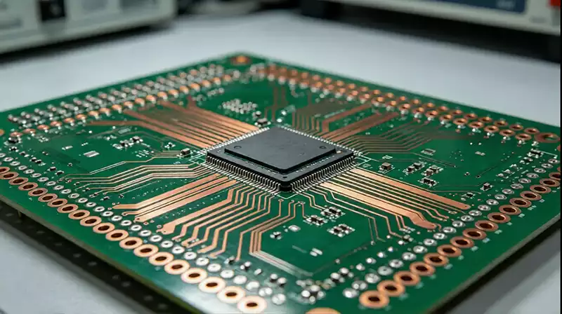
Optimizing PCB Layout for Efficient Heat Dissipation
Thermal management inside electronic equipment primarily relies on natural convection and forced airflow. Therefore, the airflow direction and cooling path of the entire system should be considered during the PCB layout design stage.
Since air naturally flows through areas with lower resistance, large empty spaces or irregular gaps on the PCB should be avoided, as they may cause unstable airflow distribution, airflow stagnation, or inefficient heat removal. For systems containing multiple PCB assemblies, all boards should follow consistent thermal layout principles to ensure smooth airflow circulation throughout the entire enclosure.
For highly temperature-sensitive core components, dedicated low-temperature operating zones should be planned in advance. These components should preferably be placed in areas with optimal cooling conditions, such as the lower section of the equipment where airflow and heat dissipation are more favorable.
They should never be installed directly above high-power heat-generating components, as thermal radiation accumulation may further increase their operating temperature. When multiple components must be installed within a limited area, staggered horizontal placement should be adopted to distribute heat sources and prevent concentrated thermal buildup.
High-power and high-temperature components should be accurately positioned in areas with the best thermal conditions inside the system, making full use of designed airflow channels and heat dissipation structures.
If no dedicated thermal management structures are available, high-temperature components should not be placed in PCB corners, edges, or other thermal dead zones where heat removal is difficult.
For conventional heating components such as power resistors, larger package sizes should be selected whenever possible to improve heat dissipation capability. During PCB layout, sufficient clearance should also be maintained around these components to avoid placing them too close to traces or neighboring devices, ensuring adequate heat spreading space.
Dedicated Thermal Management Solutions for High-Power Components
When the number of high-power heat-generating components on a PCB is limited (typically no more than three devices), an individual thermal management strategy can be adopted. Each high-power component can be equipped with a dedicated heat sink or heat pipe solution.
Under normal operating conditions, passive heat sinks are usually sufficient to maintain acceptable component temperatures. However, for extremely high-power devices where natural cooling performance is inadequate, active cooling solutions such as fan-assisted heat sinks can be implemented. Forced-air cooling significantly enhances convective heat transfer efficiency, rapidly removing excess heat and preventing localized overheating.
When the number of high-temperature components exceeds three, installing independent heat sinks for each device may result in complicated mechanical structures, excessive space consumption, and airflow interference between different cooling components. In such cases, a customized integrated heat spreader or thermal cover is generally preferred.
Based on the mounting positions, package heights, and spacing requirements of all heat-generating components, a customized flat heat spreader can be designed to cover multiple devices simultaneously. This integrated structure enables centralized heat conduction and improves overall thermal distribution efficiency.
However, due to unavoidable variations in PCB assembly processes, including soldering and component mounting tolerances, the heights of mounted components may vary slightly. As a result, the heat spreader surface may not achieve complete contact with all component surfaces, creating thermal gaps that increase thermal resistance and reduce heat transfer efficiency.
In practical engineering applications, flexible thermal interface materials (TIMs), such as phase-change thermal pads or thermally conductive gap fillers, can be installed between components and the heat spreader. These materials effectively fill microscopic gaps, reduce contact thermal resistance, and significantly improve overall thermal performance.
Improving Convection Cooling Through Optimized Component Arrangement
For electronic devices relying on natural convection cooling without forced airflow, component arrangement directly determines the efficiency of internal air circulation.
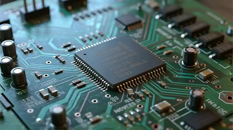
During PCB layout design, key components such as integrated circuits and power devices should follow organized horizontal or vertical placement patterns. Regular component alignment helps reduce airflow resistance, promotes stable natural convection circulation, and prevents irregular placement from blocking airflow paths or creating thermal dead zones.
By optimizing component arrangement, the PCB assembly can maximize the utilization of passive cooling mechanisms and improve the reliability of thermal management under low-airflow conditions.
Enhancing Heat Transfer Capability Through PCB Routing Optimization
The resin material within PCB substrates has extremely poor thermal conductivity and represents the primary limitation in heat transfer. In contrast, copper traces and metallic vias provide excellent thermal conductivity and serve as critical heat transfer pathways in passive PCB cooling designs.
Therefore, optimizing copper distribution and increasing the proportion of thermally conductive structures can significantly enhance the overall thermal performance of a PCB.
During PCB design, engineers can improve thermal conductivity by increasing copper area coverage, adding thermal vias where necessary, and establishing vertical heat conduction paths through multilayer PCB structures.
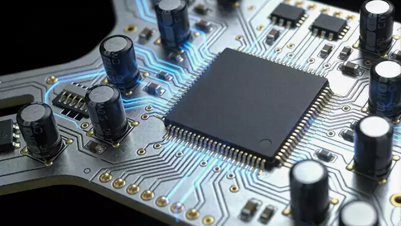
Heat generated by electronic components can then be transferred rapidly through high-conductivity copper planes and metal vias to different areas of the PCB and eventually toward board edges or external heat dissipation structures. This significantly improves heat spreading efficiency and reduces localized thermal accumulation.
A PCB is a composite structure consisting of multiple materials with significantly different thermal properties, including insulating resin, copper foil, and metallic vias. Therefore, the overall thermal performance of a PCB cannot be accurately evaluated using the thermal conductivity of a single material alone.
In engineering practice, the effective thermal conductivity of the PCB structure is commonly used as a comprehensive parameter for thermal performance evaluation. This parameter accurately reflects the overall heat transfer capability of the PCB assembly and provides reliable data support for thermal design optimization, structural adjustments, and design iterations.
Balancing PCB Power Distribution to Prevent Localized Thermal Hotspots
Uniform power distribution across the PCB is one of the fundamental principles of effective thermal management design. During the PCB design process, the overall circuit architecture should be carefully evaluated, and high-power modules and heat-generating components should be distributed appropriately to avoid excessive concentration of multiple thermal sources in a limited area.
By balancing the power density distribution across the PCB surface, designers can achieve a more uniform temperature profile and prevent the formation of localized thermal hotspots, thereby improving overall system thermal stability.
Due to limitations imposed by circuit topology, routing requirements, mechanical structures, and enclosure design, achieving completely uniform power distribution across the PCB is often impractical. However, PCB designers must strictly avoid areas with excessively concentrated power density.
Localized overheating can significantly increase the operating temperature of surrounding components, resulting in performance degradation, parameter drift, and reduced circuit stability. In severe cases, excessive thermal stress may cause short circuits, component burnout, or complete system failure.
Such thermal issues can significantly shorten the service life of electronic products and seriously compromise the reliability and operational stability of the entire electronic system.
Comprehensive PCB Thermal Design for Long-Term Reliability
PCB thermal management is not achieved through a single cooling method, but rather through a systematic engineering approach that integrates multiple design aspects, including substrate material selection, component placement optimization, airflow planning, auxiliary cooling structures, copper routing optimization, and power distribution balancing.
As electronic products continue to evolve toward higher integration density, smaller form factors, and increased power consumption, thermal design has become an increasingly critical factor in determining overall product reliability.
A well-designed PCB thermal management strategy can effectively reduce operating temperatures, improve component lifetime, enhance system stability, and ensure reliable performance under long-term operating conditions.Therefore, advanced thermal design capability and precise thermal optimization are becoming essential indicators for evaluating the reliability and competitiveness of modern electronic systems.