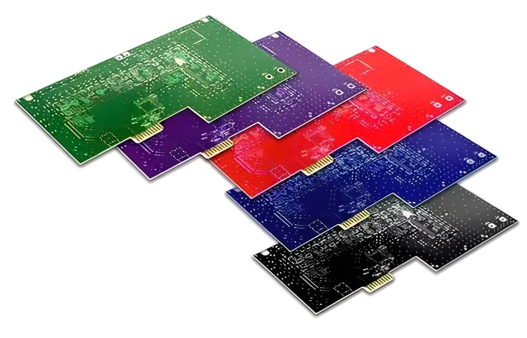
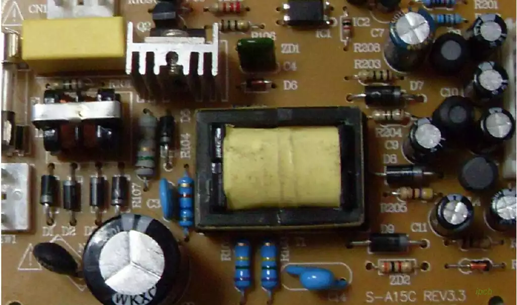
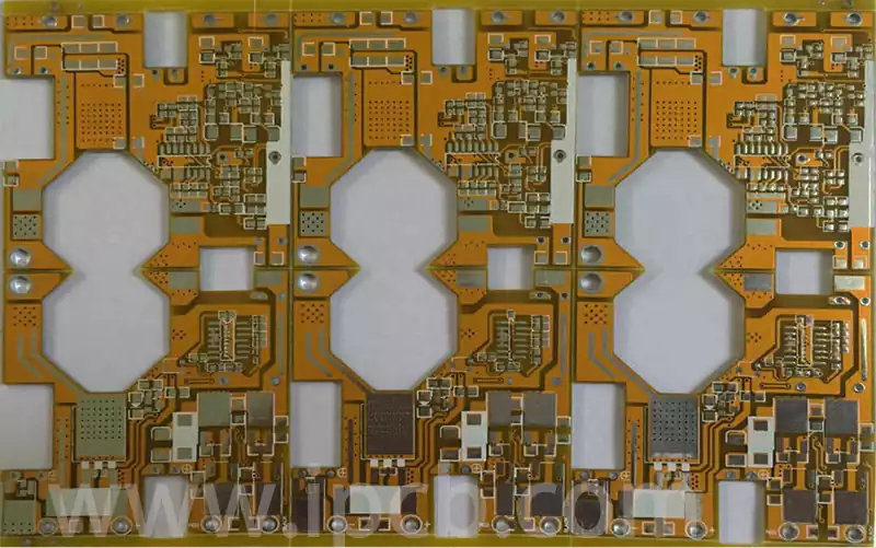
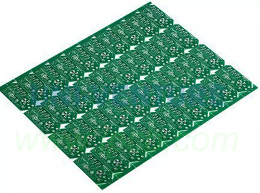
As the core carrier of electronic products, a Printed Circuit Board Assembly (PCBA) has a direct impact on product quality, operational reliability, and manufacturing yield. Whether a product can be manufactured consistently on an automated production line depends not only on the PCB design itself but also on the quality of the soldering process and the accuracy of the final assembly. For high-volume electronics manufacturing, every stage—from design and fabrication to assembly—must be planned according to Design for Manufacturability (DFM) principles to ensure compatibility with automated production equipment, minimize manufacturing defects, and maintain stable product quality.
The design stage is the foundation of the entire PCBA manufacturing process because it determines whether subsequent production can be carried out efficiently and reliably. PCB structural design should first satisfy the requirements of automated production lines by providing sufficient board-edge conveyor rails for stable transportation through SMT equipment. Proper conveyor edge design prevents board misalignment, jamming, or dropping during production. In addition, high-precision fiducial marks should be incorporated into designated locations on the PCB to provide accurate positioning references for pick-and-place machines, Automated Optical Inspection (AOI) systems, and other automated equipment, thereby ensuring precise component placement and inspection throughout the manufacturing process.
Component placement on both sides of the PCB should also be planned carefully during the design phase because the distribution of components directly affects assembly procedures, soldering processes, and equipment operation. Surface-mount devices (SMDs) and through-hole components should be arranged according to the selected manufacturing process while taking component size, package type, and mounting orientation into consideration. A well-balanced layout minimizes process conflicts between the top and bottom sides of the PCB, reduces component interference, optimizes equipment movement, and simplifies the overall assembly process, ultimately improving manufacturing efficiency.
Component placement itself requires strict compliance with manufacturing process requirements. The location, orientation, and spacing of every component should be optimized based on the intended soldering method, since reflow soldering, wave soldering, and manual soldering all have different thermal profiles and process characteristics. High-density miniature components should have sufficient spacing to facilitate heat dissipation and reliable soldering, while polarized and irregularly shaped components should maintain consistent orientation to improve assembly accuracy. Proper layout design significantly reduces the risk of insufficient solder joints, solder skips, tombstoning, and heat-related component damage during production.
Design optimization should also focus on improving soldering quality and manufacturing yield. Pad dimensions, solder mask openings, and stencil aperture designs should be carefully optimized to achieve accurate solder paste deposition while preventing solder bridging caused by excessive solder paste or insufficient solder resulting from inadequate paste volume. Components with identical package types should be arranged to ensure uniform heat distribution during reflow, allowing all solder joints within the same package to melt and solidify simultaneously for consistent solder joint quality. For plated through-hole components, via structures and hole dimensions should be designed to achieve adequate solder penetration, with a solder fill ratio of at least 75% to ensure both mechanical strength and electrical reliability.
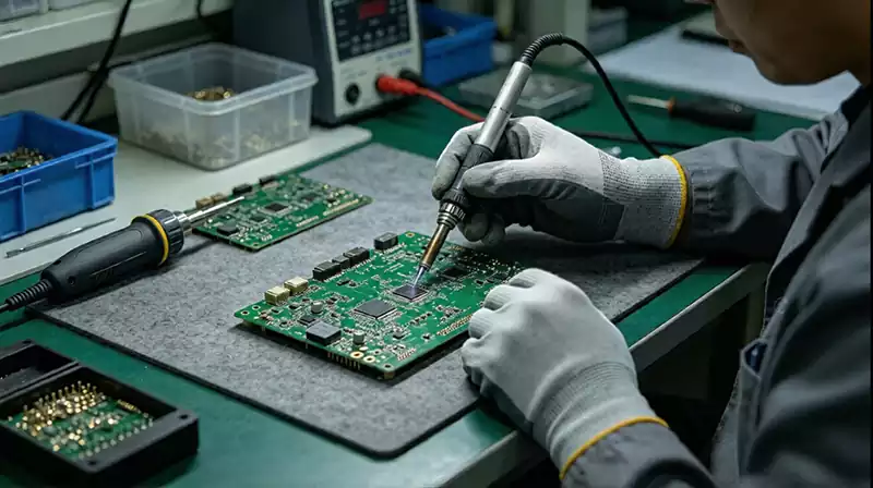
Soldering is one of the most critical stages of PCBA manufacturing, and product quality can easily be affected by electrostatic discharge (ESD), improper operating procedures, equipment failure, or process deviations. Consequently, strict ESD control should be implemented before production begins. During material handling and Incoming Quality Control (IQC) inspection, operators should wear ESD gloves at all times, all inspection instruments should be properly grounded, and ESD-safe workstations equipped with certified antistatic mats should be used throughout the production process. These measures effectively protect sensitive electronic components from latent damage caused by electrostatic discharge.
Throughout the soldering process, all components, semi-finished assemblies, and completed PCBAs should be handled and stored in ESD-safe containers rather than being placed directly on ordinary work surfaces. Every piece of soldering equipment on the production line should be properly grounded, and soldering irons should be ESD-safe models specifically designed for electronics manufacturing. Before daily production begins, equipment should undergo routine verification of insulation resistance, grounding continuity, and ESD performance to eliminate failures caused by electrical leakage or accumulated static electricity.
After wave soldering, special attention should be given to the alignment of through-hole components. During the soldering process, molten solder flow may exert mechanical force on component leads, causing components to shift or tilt from their intended positions. Misaligned components may extend beyond the silkscreen outline, negatively affecting product appearance while also creating potential assembly interference and electrical connection issues. Therefore, all through-hole components should be visually inspected after wave soldering, and any displaced components should be corrected immediately to ensure proper installation accuracy.
Certain components, including speakers and batteries, require particularly careful control of solder volume during manual soldering or touch-up operations. Excessive solder may create bridges between adjacent terminals, resulting in electrical short circuits, poor mechanical stability, or component detachment. The amount of solder applied should therefore be precisely controlled to produce smooth, well-formed solder joints without excess solder, cold joints, or insufficient wetting while maintaining both mechanical integrity and electrical reliability.
Proper storage of bare PCBs is equally important throughout the manufacturing process. Bare boards should be arranged neatly without direct stacking to prevent scratches on copper traces or solder pads. Whenever multiple boards must be stored together, each PCB should first be sealed inside an ESD shielding bag before stacking to protect it from dust contamination, electrostatic discharge, and mechanical damage.
Final product assembly represents the last stage of PCBA manufacturing and plays a decisive role in determining overall product quality and shipment yield. Even during final assembly, strict ESD protection should remain in place. Semi-finished products without protective enclosures should always be stored in ESD shielding bags to prevent electrostatic discharge and airborne contamination from damaging exposed electronic circuits. At the same time, manufacturers should routinely inspect all ESD protection equipment, tools, and consumable materials to ensure that the entire production environment continues to meet established ESD control standards.
A standardized production workflow is equally important for maintaining product consistency. Under normal manufacturing conditions, the process follows a fixed sequence beginning with material release from the warehouse, followed by material loading onto the production line, firmware programming, mechanical assembly, initial functional testing by Quality Control (QC), IMEI programming, comprehensive Quality Assurance (QA) inspection, restoration of factory settings, and finally finished goods warehousing. Firmware programming is a particularly critical step because it must be completed before final mechanical assembly. Once the product enclosure has been fully assembled, firmware downloading or upgrading is generally no longer possible.
Throughout the manufacturing process, every potential source of failure should be carefully controlled. Defects such as poor solder joints, electrical short circuits, or improper production operations may all lead to firmware programming failures, which can easily be misidentified as defective products. Maintaining strict control over soldering quality, manufacturing procedures, and inspection at every production stage allows manufacturers to accurately identify the root causes of failures, reduce false rejection rates, improve manufacturing yield, and ensure consistent product quality.
PCBA manufacturing is a highly integrated engineering process in which every stage is closely interconnected. Design for manufacturability establishes the foundation for efficient production, standardized soldering processes minimize manufacturing defects, and disciplined assembly and inspection ensure the quality of the finished product. By following proven design guidelines, standardized manufacturing procedures, and comprehensive quality control practices, manufacturers can significantly reduce production defects, improve soldering reliability and overall yield, and consistently deliver high-quality PCBAs that satisfy the requirements of modern industrial-scale electronics manufacturing.