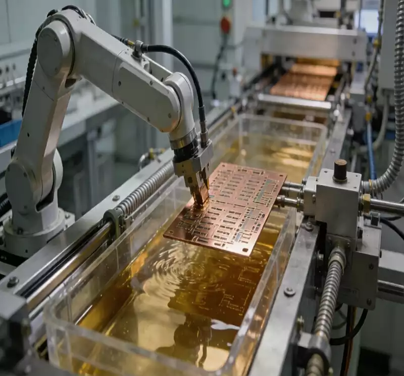
mSAP (Modified Semi-Additive Process) is a high-precision manufacturing technology designed for High-Density Interconnect (HDI) PCBs.
Its core principle is ‘seed copper plating + selective etching’. By adopting an ‘additive’ approach—the opposite of the traditional subtractive method—it achieves fine-line processing: an ultra-thin copper foil, just 3μm thick, is bonded to the substrate; photoresist is used to pattern the circuit; the target areas are selectively plated to thicken them; and finally, the excess copper layer is stripped away.
This method effectively avoids the lateral corrosion associated with etching, enabling line width precision to leap from the conventional 50μm to 10μm—equivalent to etching a complex circuit spanning kilometres onto an area the size of a fingernail. Currently, mSAP can consistently achieve a processing capability of 15μm line width/spacing. By controlling the distance between the circuit lines and the reference plane to <10μm, coplanar waveguide loss can be reduced by 20%, significantly improving signal integrity in the millimetre-wave band.
Technical Features
High precision: Line width tolerance of ±3 μm, superior to the ±8 μm achieved by the subtractive method.
High material utilisation: Copper foil utilisation increased from 55% in the subtractive method to 92%.
Excellent signal integrity: Impedance control accuracy of ±5%, suitable for 56 Gbps+ high-speed signal transmission.
Environmental Benefits: Reduced etching steps and the adoption of a cyanide-free process result in a 60% reduction in wastewater treatment costs.
The three stages of mASP technology development
Stage 1 (1990s–early 2000s): The era of traditional subtractive processes
Early HDI boards were based on subtractive or printed etching processes, combined with traditional core-on-core and sequential lamination, enabling the production of circuit boards with line widths and line spacings of approximately 60 μm. High-density interconnections were primarily achieved through microvias.
Stage Two (Early 2000s–Mid-2010s): The Development of Any-Layer Technology
With the rise of smartphones, the second generation of HDI emerged. Whilst retaining laser-drilled microvias, stacked vias gradually replaced staggered vias. Combined with ‘any-layer’ construction technology, line widths and spacing reached 40μm. Subtractive processes remained the mainstream technology during this phase.
Phase Three (mid-2010s to present): The mSAP Process Revolution
The year 2017 marked a pivotal turning point—Apple’s iPhone motherboards began adopting Substrate-Like PCBs (SLP), driving the shift in HDI from the subtractive method to mSAP. The semi-additive process (SAP) can process lines of <15μm and is primarily used for packaging substrates; meanwhile, the modified semi-additive process (mSAP) and its advanced version (amSAP) have become the core processes for next-generation HDI PCBs.
The Core Value of the mSAP Process
Precision: Enables the mass production of fine-line circuits, consistently achieving 10μm line width and spacing, with high-end products reaching the 5μm level and line width tolerances controlled within ±1μm. Compared to the subtractive method, circuit density is increased threefold, and the volume of smartphone motherboards can be reduced to 70% of the original size, freeing up more space for modules such as batteries and cameras.
Efficiency and Cost: Balancing mass-production feasibility with economic viability. Compared to the full additive method, production efficiency is improved by over 30%, whilst maintaining a yield rate of over 90%; compared to the subtractive method, copper material utilisation reaches 92%, reducing copper waste by 60%, whilst simultaneously lowering etchant consumption and waste liquid treatment costs. Taking high frequency ceramic substrates as an example, the traditional subtractive method requires 35μm copper foil, whereas mSAP requires only a 0.3μm seed layer, resulting in a 70% reduction in material costs.
Adaptability: Wide range of applications, meeting the stringent demands of high-end sectors.
High-speed optical modules (400G/800G): The low-roughness copper surface reduces high-frequency losses, whilst precise impedance control prevents signal crosstalk.
High-end semiconductor packaging: Supports 0.4mm pitch BGA packaging, suitable for high-density interconnects in 3nm chips.
Automotive electronics (Level 4 autonomous driving): Supports multi-camera and radar data transmission with signal latency <2ns.
5G Communications: Supports 64T64R massive MIMO antenna arrays, meeting transmission requirements for the 28GHz millimetre-wave band.
Furthermore, the mSAP process is seamlessly compatible with technologies such as laser drilling, Automated Optical Inspection (AOI) and embedded component integration. It supports microvia processing and 3D stacking designs, offering greater design freedom for innovative products.
Technical Improvements in Core Process Steps
1.Substrate Processing
The key lies in the application of ultra-thin copper foil (1–3 μm) to reduce etching side-etching. Carrier copper foil technology (such as Mitsui Metal’s MT12GN, which uses a 12 μm copper foil carrier) makes the processing of ultra-thin copper foil more stable, helping to improve laser drilling quality.
2.Pattern Transfer
Laser Direct Imaging (LDI) technology is primarily employed. Han’s Laser’s CO₂ laser drilling machines achieve a precision of 50 μm, whilst ultra-fast laser solutions break the 30 μm barrier. Ultra-short pulse (USP) lasers (picosecond/femtosecond class) can create smaller through-holes and heat-affected zones, significantly reducing the pitch of microvias. The Mitsubishi CO₂ laser machine ML605GTWIV-H, by coordinating table movement with laser processing, reduces movement time by approximately 70% and increases production efficiency by 35%.
3.Electroplating Innovations
Vertical continuous electroplating equipment utilises pulse electroplating technology, achieving uniformity of 25 μm ± 2.5 μm (plate thickness 0.1–3.0 mm), with a through-hole rate of ≥85% at an aspect ratio of 8:1. The MVCP hole-filling electroplating equipment (specifically designed for mSAP) achieves 98% copper uniformity within the holes.
4.Etching Optimisation
Rapid flash etching technology is employed to achieve vertical sidewalls. As the carrier substrate consists of ultra thin copper foil with extremely low roughness (Rz 0.8–3.0 μm) and minimal thickness (1.5–5.0 μm), the cross-section of the circuit after etching is rectangular, resulting in a high etch factor that meets the requirements for vertical sidewalls.
The mSAP process strikes an effective balance between precision, efficiency, cost and environmental sustainability,providing a mature and reliable technical pathway for the mass production of high density interconnect (HDI) PCBs.