PCB level shielding refers to design techniques that utilize multiple shielding methods within the internal structure, trace layering, grounding layout, and localized metal shielding of printed circuit boards (PCBs) to reduce electromagnetic interference (EMI) and enhance electromagnetic compatibility (EMC).
The objective of PCB level shielding is to employ a series of technical measures to reduce or prevent the propagation of electromagnetic interference between different sections of the circuit board and between the board and its external environment, thereby ensuring the stable and reliable operation of electronic equipment. This is manifested in the following key aspects:
Ensuring Stable Circuit Performance
Preventing signal distortion: Circuits on a PCB generate electromagnetic signals of varying frequencies and intensities during operation. Mutual interference—particularly when high-speed digital signals disrupt sensitive analog signals—can cause waveform distortion and signal degradation. For instance, in audio processing circuits, high-frequency noise from digital circuits coupling into analog audio signals introduces audible noise. PCB level shielding effectively isolates different circuit modules, reducing signal interference to ensure accurate transmission and processing, thereby maintaining stable circuit performance.
Maintaining stable operating frequencies: For circuits demanding high frequency stability, such as oscillators and clock circuits, external electromagnetic interference can affect oscillation frequencies, causing frequency drift. In communication equipment, for instance, clock frequency drift impacts data synchronization and transmission quality. PCB level shielding blocks external interference, maintaining stable operating frequencies for such circuits and ensuring proper device function.
Enhancing Equipment Interference Resistance
Resisting External Electromagnetic Environmental Interference: The external environment surrounding electronic equipment contains numerous sources of electromagnetic interference, such as radio broadcasts, communication base stations, high-voltage transmission lines, and lightning. The electromagnetic waves generated by these sources may enter the circuit board through spatial radiation or conduction, affecting normal circuit operation. For instance, in industrial control systems, strong electromagnetic interference generated by large motors or welding machines can cause control circuit malfunctions without effective shielding measures. PCB level shielding creates an electromagnetic barrier that blocks external interference, enhancing equipment adaptability in complex electromagnetic environments.
Enhancing Equipment Reliability in Harsh Conditions:
In extreme environments like high temperatures, humidity, or intense vibration, electronic devices’ electromagnetic compatibility may be compromised. PCB level shielding not only provides electromagnetic protection but also shields circuit boards from environmental factors to some extent. For instance, sealed shielding enclosures prevent moisture and dust from entering the circuit board interior, reducing circuit failures caused by environmental factors and improving equipment reliability in harsh conditions.
Meeting Electromagnetic Compatibility Standards
Compliance with Regulatory Requirements: To ensure global sales and use of electronic devices, countries have established stringent Electromagnetic Compatibility (EMC) standards and regulations. These clearly define limits for electromagnetic radiation emitted by electronic equipment and specify requirements for interference immunity. PCB level shielding serves as a critical technical measure to meet these standards and regulations. Through proper shielding design, electromagnetic radiation levels from the circuit board can be controlled to remain below specified limits while enhancing the device’s immunity to interference. This ensures the equipment successfully passes relevant certifications and testing for market entry.
Avoiding EMC Disputes: If an electronic device generates electromagnetic interference exceeding specified limits, it may disrupt other nearby electronic equipment, leading to disputes. For instance, in hospitals, electromagnetic interference from medical devices could affect the proper functioning of critical medical equipment, potentially endangering patient safety. Effective PCB level shielding reduces the electromagnetic radiation emitted by devices, preventing disputes and legal liabilities arising from EMC issues.
Optimizing Overall Device Design
Enabling Miniaturization and Integration: With advancing electronic technology, devices are trending toward miniaturization and integration. As PCB component density increases and layouts become more compact, electromagnetic interference issues become more pronounced. PCB level shielding technology enables efficient electromagnetic protection within limited space without compromising miniaturization or integration. For instance, multi-layer shielding structures and micro-shielding enclosures can effectively isolate different circuit modules without increasing device volume, enhancing overall electromagnetic compatibility.
Reducing Design Costs and Cycle Times: Well-planned PCB level shielding addresses EMC issues early in the design phase, avoiding extensive later modifications and debugging. This lowers design costs, shortens development cycles, and accelerates time-to-market. For instance, using simulation software during design to analyze PCB EMC and optimize shielding based on results reduces the need for physical testing and associated expenses.
Design Considerations for PCB-Level Shielding
Shielding Zone Planning
Identify Sensitive Areas: Pinpoint circuits on the PCB susceptible to electromagnetic interference (EMI), such as analog signal processing circuits, high-frequency small-signal amplification circuits, and low-level measurement circuits. These circuits are highly sensitive to EMI, where even minor interference can cause signal distortion or measurement errors. For example, in audio processing circuits, analog audio signals have low amplitudes and are susceptible to high-frequency noise generated by digital circuits. Therefore, the analog audio processing section should be designated as a sensitive area requiring focused shielding.
Identify interference source areas: Locate circuit modules on the PCB that generate strong electromagnetic interference, such as high-speed digital circuits, switching power supply circuits, and high-power RF circuits. These circuits produce significant electromagnetic radiation and conducted interference during operation, potentially affecting other circuits. For instance, clock signals in high-speed digital circuits feature high frequencies and steep edge rates, generating strong electromagnetic radiation. They must be isolated from other sensitive circuits.
Optimize Component Layout: Based on the delineation of sensitive and interference-source zones, arrange components and circuits on the PCB rationally. Position sensitive circuits as far as possible from interference sources to minimize coupling paths. For instance, separate analog and digital circuits into distinct PCB regions, divided by shielding layers or isolation strips.
Shielding Structure Optimization
Ensure Shielding Continuity: Maintain uninterrupted shielding layers, eliminating gaps and holes. Gaps and holes become leakage paths for electromagnetic interference, degrading shielding effectiveness. For instance, when using metal shielding enclosures, ensure tight contact between the enclosure and PCB with no gaps. For metal shielding layers in multilayer PCBs, guarantee reliable connections between layers to form a complete shielded cavity.
Implementing Multilayer Shielding: For PCBs with stringent electromagnetic compatibility requirements, adopt multilayer shielding structures. Multi-layer shielding further enhances shielding effectiveness and reduces electromagnetic interference penetration. For example, in multilayer PCBs containing high-speed digital circuits and high-frequency analog circuits, metal shielding layers can be placed between different signal layers to form multiple independent shielded cavities, isolating electromagnetic interference between distinct signal layers.
Optimize shielding enclosure design: When using shielding enclosures, the shape and dimensions should be reasonably designed. The shield should fully cover the area requiring protection while considering heat dissipation and installation convenience. For instance, ventilation holes can be incorporated into the shield, but their size and distribution must be carefully managed to prevent excessive holes from compromising shielding effectiveness.
Grounding Design
Selecting Appropriate Grounding Methods: Common grounding approaches include single-point grounding, multi-point grounding, and hybrid grounding. Single-point grounding is suitable for low-frequency circuits, preventing ground loop interference. Multi-point grounding is suitable for high-frequency circuits, reducing ground impedance. Hybrid grounding combines the advantages of both single-point and multi-point grounding, making it suitable for complex circuits containing both low-frequency and high-frequency signals. For example, single-point grounding can be used in low-frequency analog circuits, while multi-point grounding is preferable in high-speed digital circuits.
Ensure proper grounding: The shield ground connection must be reliable with minimal ground resistance. Poor grounding degrades shielding effectiveness and may even generate new electromagnetic interference. For example, when grounding a metal shield, use conductive fasteners like screws or spring clips to ensure a solid electrical connection between the shield and ground.
Avoid ground loops: Ground loops occur when multiple ground paths exist in a circuit. Current flowing through these paths generates magnetic fields, introducing electromagnetic interference. When designing shield grounding, minimize the formation of ground loops. Methods include employing single-point grounding or using isolation transformers to break ground loops.
Thermal Considerations
Assessing the impact of shielding on heat dissipation: While shielding structures block electromagnetic interference, they may also impede heat dissipation from circuit boards. For instance, metal shielding enclosures can obstruct heat dispersion, leading to elevated board temperatures. Therefore, when designing shielding, evaluate its thermal implications to ensure the circuit board maintains adequate heat dissipation during operation.
Designing Heat Dissipation Pathways: To resolve the conflict between shielding and heat dissipation, appropriate heat dissipation pathways can be incorporated. For instance, ventilation holes may be incorporated into the shielding enclosure, though care must be taken regarding their size and distribution to prevent excessive shielding effectiveness loss due to overly large or numerous openings. Alternatively, shielding enclosures may be fabricated from metals with favourable thermal conductivity, supplemented with heat sinks or fans mounted on the enclosure.
Material Selection
Select materials based on shielding requirements: Different shielding materials exhibit varying electromagnetic shielding properties and physical characteristics. When choosing shielding materials, consider the circuit board’s shielding requirements and operating environment. For instance, materials with high electrical conductivity and magnetic permeability, such as copper or aluminium, should be selected for high-frequency electromagnetic interference. For shielding structures subjected to significant mechanical stress, higher-strength materials like stainless steel are preferable.
Consider material cost and processability: Beyond shielding performance, account for material cost and machinability. Selecting moderately priced, easily processed materials reduces PCB manufacturing expenses. Copper foil, for instance, is a common shielding material offering excellent conductivity and workability at relatively low cost.
Balancing Cost and Manufacturability
Controlling shielding costs: Shielding design should minimise expenditure while meeting electromagnetic compatibility requirements. Cost-effective shielding measures such as shielding coatings or localised shielding may be employed instead of relying solely on expensive full enclosures. Simultaneously, optimise shielding structures to minimise material usage and reduce manufacturing expenses.
Ensuring manufacturability: Shielding designs must account for PCB manufacturing and assembly processes to ensure structures are readily producible and installable. For instance, when designing shield enclosures, consider their mounting and fixation methods relative to the PCB to prevent assembly difficulties or diminished shielding effectiveness due to poor design.
PCB level shielding methods:
- Ground Plane Shielding
Incorporating a continuous GND layer within the PCB serves to:
Provide a low-impedance path
Absorb interference
Reduce loop area to minimise radiation
This constitutes the most fundamental PCB shielding technique. - Multilayer Stack-up Shielding
Example:
Inner layers carry high-speed signals (Stripline)
Outer layers function as shielding planes
GND/POWER layers tightly coupled
The stack-up structure encloses high-speed signals within metal layers, enhancing shielding efficacy. - Via Shield Fence (or Via Stitching)
Dense ground vias placed around sensitive traces or modules form a metallic ‘wall’:
Function:
Block lateral electromagnetic wave propagation
Locally isolate RF, power supply, and clock domains
Widely employed in RF and high-speed designs.
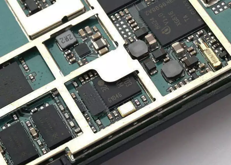
- Localised Metal Shielding Can
Installing a metal enclosure over high-interference areas such as RF, clock, or power zones to create a Faraday cage-like structure.
Function:
Provides robust shielding against electromagnetic radiation
Prevents interference with sensitive circuits
- Differential Pair Shielding, Ground Shielding, Mesh Shielding, etc.
Examples:
Placing ground shields between high-speed traces
Employing mesh ground planes
Enhancing return path integrity
These also constitute PCB level shielding techniques.
PCB level shielding plays an indispensable role in ensuring the stable operation of electronic equipment. From defining its primary objectives to mastering design principles, each element is interconnected and mutually influential. Only through comprehensive and in-depth understanding and application of this knowledge can efficient electromagnetic shielding be achieved in PCB design. This enables the creation of stable-performing, interference-resistant, standards-compliant, and optimally designed electronic devices, thereby driving the continuous advancement of electronic technology.