A high frequency antenna operates in the 300 MHz–300 GHz RF spectrum (corresponding to electromagnetic wavelengths of 1 m–1 mm). It is the core RF component responsible for bidirectional energy conversion between guided high-frequency electrical signals and free-space electromagnetic waves. High-frequency antennas serve as the transmission and reception “gateway” in wireless communication, radar, positioning, and remote sensing systems. They are also among the most process-sensitive modules in PCB RF design and manufacturing.
Classification of High Frequency Antennas
Ultra High Frequency (UHF, 300 MHz–3 GHz)
An entry-level high-frequency band widely used in industry. Typical examples include 2.4 GHz Bluetooth, WiFi, Zigbee antennas, RFID antennas, and remote-control antennas. This band dominates consumer electronics and general IoT applications. PCB process tolerances must meet baseline precision requirements.
Super High Frequency (SHF, 3 GHz–30 GHz)
The mainstream commercial high-frequency band, covering 5G Sub-6 GHz, WiFi 6/7, automotive V2X, and industrial wireless gateways. It represents the core track of modern high-frequency PCB manufacturing, requiring strict impedance control, solder mask uniformity, and trace accuracy.
Extremely High Frequency (EHF, 30 GHz–300 GHz, Millimeter Wave)
A high-end frequency band used in 5G mmWave, 77 GHz automotive collision-avoidance radar, satellite communications, and early-stage 6G research. As wavelengths shrink to millimeter scale, even micron-level PCB deviations—such as solder mask thickness variation or trace misalignment—can cause antenna performance failure.
Operating Principles of High Frequency Antennas
Transmit Mode:
High-frequency alternating current from the RF chip is converted by the radiating element into electromagnetic waves that propagate freely in space, enabling wireless transmission.
Receive Mode:
The antenna captures incoming electromagnetic waves and converts them into high-frequency electrical signals that can be recognized and processed by the RF front-end circuitry.
Types of PCB Mounted High Frequency Antennas
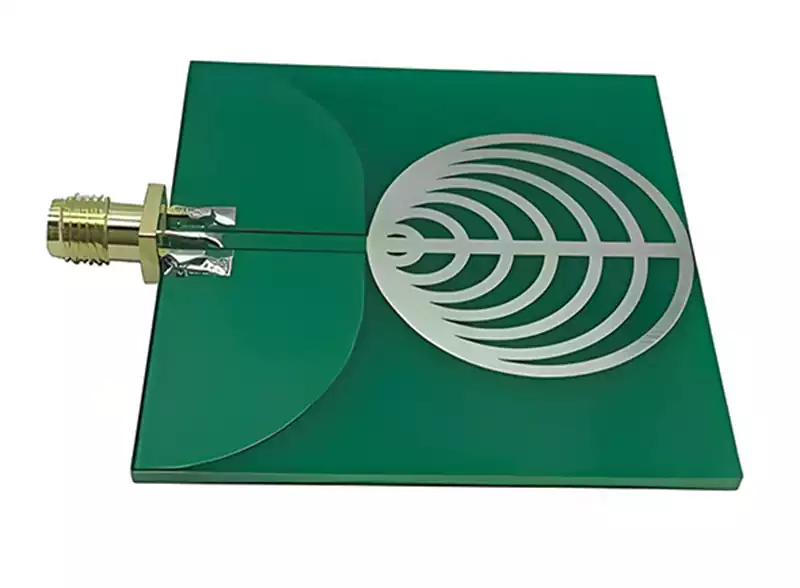
Microstrip Patch Antennas
The dominant structure for millimeter-wave array antennas and 5G terminal antennas. They feature a low profile and easy integration, but demand extremely high consistency in PCB substrate and solder mask properties.
IFA / PIFA Antennas
Classic solutions for smartphones and smart home devices, balancing miniaturization with omnidirectional radiation performance.
Dipole / Inverted-F Antennas
Widely used in Bluetooth and WiFi modules. Simple in structure but highly sensitive to impedance matching accuracy.
Antenna Arrays
Core solutions for automotive radar and small-cell base stations. Multiple radiating elements cooperate to enhance gain and directivity. They require exceptionally tight batch-to-batch manufacturing consistency.
How the Solder Mask Affects High Frequency Antenna Performance
1.Resonant Frequency Shift and Bandwidth Reduction
The resonant frequency of an antenna is determined by the radiator dimensions, substrate effective dielectric constant, and surrounding medium.
Applying solder mask is equivalent to adding a high-dielectric layer above the antenna surface, increasing the effective dielectric constant and slowing electromagnetic wave propagation. As a result, the resonant frequency shifts downward.
The shift typically ranges from 3%–10%, with greater impact at higher frequencies. In millimeter-wave antennas—where structures are compact and bandwidths narrow—even slight shifts can significantly degrade impedance matching, gain, and radiation efficiency.
2.Impedance Mismatch and Increased Signal Reflection
50 Ω is the standard impedance for RF transmission lines. After applying conventional solder mask, the effective dielectric constant of microstrip lines increases, reducing characteristic impedance—often to 45–48 Ω—creating impedance discontinuities.
This leads to increased reflections, degraded return loss (S11), and higher VSWR. Energy that cannot radiate effectively is converted into heat and noise.
A thickness variation of ±5 μm may cause impedance fluctuation of ±2–3 Ω, which is sufficient to cause module failure above 24 GHz.
3.Increased Insertion Loss and Reduced Radiation Efficiency
Due to the skin effect, high-frequency current concentrates within the top 0.5–3 μm of the conductor surface. Solder mask directly covers this current path, introducing additional dielectric and conductor losses.
Loss increases with frequency. At 28 GHz, attenuation may rise by 0.3–0.8 dB per centimeter. Long-term coverage can reduce antenna efficiency by 5%–15%, directly affecting communication distance, sensitivity, and interference immunity.
4.Process Tolerances Amplify Performance Variations
Typical solder mask thickness ranges from 10–30 μm, with uniformity of ±5–10 μm, and inherent edge-profile and alignment tolerances.
While negligible at lower frequencies, these small variations are magnified at millimeter-wave frequencies, resulting in batch performance dispersion.
Consequences include radiation pattern distortion, operating frequency drift, and poor production consistency—raising debugging and mass-production costs.
Core Solutions for High Frequency Antenna Solder Mask Design
1.Solder Mask Opening in Antenna Regions (Preferred Solution)
The most direct and effective approach is to open windows over the antenna radiator, feedline, and impedance matching sections, eliminating dielectric interference from the solder mask.
Design Guidelines:
Extend the opening 0.1–0.2 mm beyond the copper outline to compensate for alignment tolerances
Use rounded edges to prevent field concentration and additional loss
Ensure no ink residue; apply plasma cleaning for surface cleanliness
Recommend ENIG (Electroless Nickel Immersion Gold) surface finish with gold thickness controlled at 0.05–0.1 μm to minimize conductor loss
This approach virtually eliminates resonant shift and impedance drift, restoring antenna efficiency to over 95% of theoretical values. It is the preferred solution for automotive radar and high-precision RF modules.
2.Use Low-Dk/Df High-Frequency Solder Mask When Coverage Is Required
In waterproof, dustproof, or chemical-resistant applications where solder mask coverage is mandatory, conventional inks should be replaced with high-frequency-grade solder mask materials:
Dk ≤ 3.2, Df ≤ 0.015, stable at 10 GHz
Thickness controlled at 5–10 μm, uniformity within ±3 μm
Low moisture absorption and low volatility
Prefer matte green to reduce pigment-induced dielectric variation
Material upgrades can reduce loss by 30%–50% and limit frequency shift to within 2%, achieving a balance between protection and RF performance for consumer and industrial applications.
3.Impedance Pre-Compensation and Simulation-Driven Design
During the design stage, solder mask must be included as a structural layer in EM simulation. Tools such as HFSS, CST, and ADS should be used to build a complete stack-up model including:
Solder mask type and Dk/Df parameters
Actual thickness and uniformity
Surface roughness
Surface finish type
Based on simulation results, impedance pre-compensation can be applied. When solder mask is present, trace width may be slightly reduced to offset impedance decrease caused by increased dielectric constant, ensuring final impedance falls within 50 Ω ±1 Ω.
Typical compensation ranges from 5%–10%, depending on material and thickness.
4.Precision Manufacturing Control
Antenna performance depends equally on design and manufacturing quality. Critical control points include:
LDI (Laser Direct Imaging) with alignment accuracy of ±0.01 mm
Closed-loop solder mask thickness control with in-line monitoring
50× microscopic inspection of solder mask openings (residue area ≤1%)
Plasma cleaning to remove residual adhesives and organic contaminants
Finished product impedance and S-parameter testing for consistency
Stable process control can limit batch performance deviation to within 5%, meeting automotive and telecom-grade reliability standards.
5.Structural and Layout Optimization
Avoid solder mask bridges, brackets, or markings in antenna regions
Maintain ≥0.3 mm spacing between solder mask edges and antenna elements
Keep large ground and shielding structures open to reduce parasitic effects
Avoid silkscreen markings on radiating surfaces and feedline areas
Optimized layout further reduces stray losses and improves radiation pattern integrity.
As wireless communication continues evolving toward higher frequencies and greater miniaturization, the performance ceiling of high-frequency antennas is no longer determined solely by radiator design. It is increasingly influenced by seemingly basic structural details such as the solder mask layer.
In the current era of continuous advancement towards higher frequencies and miniaturisation in wireless communication technology, the performance ceiling of high frequency antennas is no longer solely determined by the design of the radiating elements. Instead, it lies concealed within seemingly fundamental structural details such as the solder mask.
From resonant frequency shifts to impedance mismatches, from increased insertion loss to mass production performance variability, the impact of solder mask layers on the electrical characteristics of high frequency antennas intensifies with increasing frequency bands. This makes them an unavoidable core issue in the implementation of RF products.