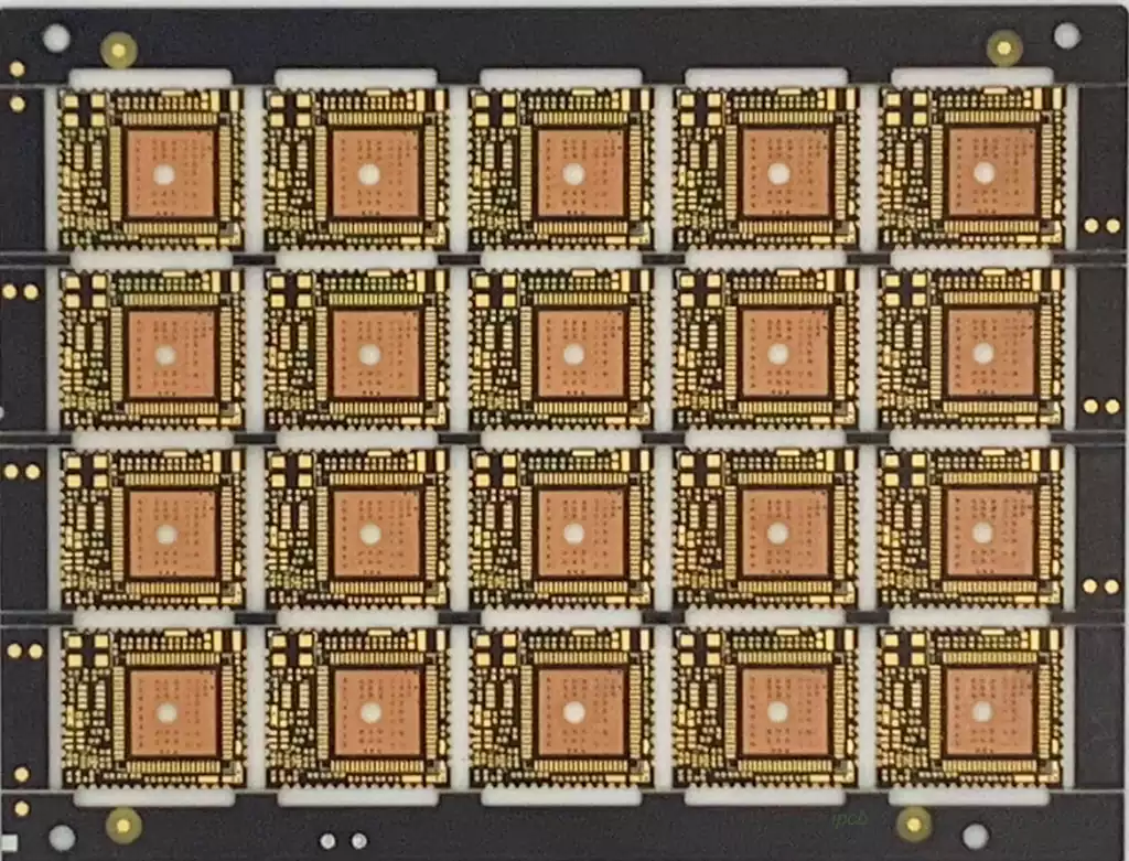
OSP (Organic Solderability Preservative) is a surface treatment process for PCBs (Printed Circuit Boards). It involves coating the copper foil surface with an extremely thin organic protective film (approximately 0.2-0.5μm thick) to prevent copper oxidation and maintain solderability. During soldering, high temperatures cause the protective film to decompose, exposing the copper surface to bond with the solder, thereby achieving excellent soldering results.
Purpose of OSP Surface Treatment
The primary objective of OSP surface treatment is to form an oxidation-resistant protective layer on PCB substrates, thereby enhancing product reliability and stability. Additionally, this process minimises adverse effects on subsequent operations such as drilling and assembly.
General PCB OSP Process Flow:
- Substrate Preparation: The PCB substrate to be treated must first be prepared. Ensure the substrate surface is smooth, free from contamination, and undergoes necessary pre-treatment, such as deoxidation and cleaning.
- Chemical Cleaning: The PCB undergoes chemical cleaning to remove surface contaminants, oils, and other impurities. Common cleaning methods include acid washing, alkaline washing, and deionised water rinsing.
- Promoter Application: Following cleaning, a layer of Organic Solderability Preservative promoter is applied to the PCB surface. This promoter enhances surface wettability and solderability of the pads, thereby improving soldering reliability.
- Baking: The PCB coated with Organic Solderability Preservative promoter undergoes high-temperature baking to firmly adhere the promoter to the pad surface and form a protective film. Baking temperature and duration are determined according to the specific promoter and PCB requirements.
- Inspection and Repair: OSP-treated PCBs undergo inspection to verify the protective film quality meets specifications. Defective or non-compliant areas require repair or reapplication of coating and baking steps.
- Packaging and Delivery: Finally, PCBs processed through the OSP procedure are packaged and delivered according to customer requirements.
Process Requirements for OSP Surface Treatment
(1) Cleaning Requirements: Cleaning constitutes the initial stage of the Organic Solderability Preservative surface treatment process, with its efficacy directly impacting the quality and performance of subsequent operations. Consequently, cleaning agents employed must demonstrate excellent capabilities in removing grease, dust, and other contaminants, whilst also exhibiting low toxicity and environmental compatibility.
(2) Pre-treatment Requirements: Pre-treatment removes oxidation layers and other contaminants from the PCB surface to enhance OSP effectiveness. Chemical cleaners and oxidation removers must be employed during this stage to achieve the desired outcome.
(3) OSP Solution Treatment Requirements: OSP solution treatment constitutes the core process, directly influencing PCB surface quality and performance. Consequently, parameters such as temperature, concentration, and duration of the OSP solution must be strictly controlled to ensure the formation of a uniform, dense protective layer on the PCB surface.
(4) Drying Requirements: Drying serves to eliminate excess moisture and solvents from the PCB surface, thereby safeguarding surface quality and performance. Appropriate drying equipment and methods must be employed during this process to ensure moisture and solvent content on the PCB surface meet specified standards.
(5) Inspection Requirements: Inspection constitutes a critical stage in verifying that the PCB surface quality and performance meet specifications. Consequently, inspectors must possess proficient inspection skills and equipment, alongside established rigorous inspection standards and methodologies to guarantee product quality and performance.
Characteristics of OSP
The freshly exposed copper surface of PCB pads is highly susceptible to oxidation, forming a layer that impedes soldering. Thus, a heat-resistant, oxidation-inhibiting protective measure is essential. OSP achieves this by forming robust complexes with fresh copper through highly reactive imidazole compounds. These complexes possess a moderate thickness of approximately 0.2–0.5 μm, effectively preventing oxidation and contamination even under heated conditions. This complex demonstrates exceptional performance in the high-temperature environment of lead-free soldering, exhibiting no decomposition or gas evolution. Currently, OSP formulations utilising alkylphenyl imidazole derivatives with superior thermal stability are highly favoured. Their thermal decomposition temperature reaches 354.7°C, significantly enhancing heat resistance and making them ideal for applications involving multiple reflow cycles in lead-free soldering. OSP not only provides robust protection and high-temperature resistance but also exhibits excellent solderability at elevated temperatures.
Influencing Factors and Countermeasures
The core of the OSP process lies in precisely controlling the thickness of the anti-oxidation film. Parameters such as the pH value and acidity of the bath solution directly affect film thickness and require regulation to ensure process effectiveness. Maintaining the film thickness between 0.2 and 0.5 micrometres is considered the optimal range, with the ideal thickness set at 0.35 micrometres. Both excessively thin and excessively thick films can adversely affect the process. Additionally, attention must be paid to the uniformity of micro-etching on the copper surface, the critical importance of post-treatment rinsing, and the significance of air-drying.
OSP boards must be stored in a low-temperature, low-humidity environment, with temperatures controlled between 15-25°C to prevent damage from excessive heat or cold. Regarding humidity, the relative humidity of the storage environment should not exceed 60% to guard against moisture affecting board performance. Furthermore, at the SMT site, a series of operational procedures must be followed to ensure the performance and quality of OSP boards remain unaffected. Following unpacking, assembly should commence within 48 hours. Once assembled, the DIP process should be performed within 24 hours.
The OSP surface treatment provides reliable oxidation resistance and solderability for PCBs. However, meticulous control of process parameters and strict adherence to operational procedures are essential. Optimising storage conditions and minimising the time between unpacking and use are crucial for maintaining stable performance, thereby supporting high-quality production of electronic products.