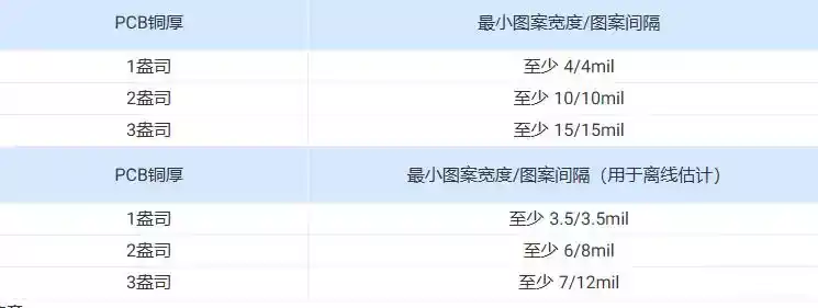
PCB board copper thicknesses are generally classified as 1oz (35μm), 2oz (70μm) and 3oz (105μm). Of course, the copper thickness depends on the type of board you are making. Copper thickness for switching power supplies with high currents is 2oz. for signal transmission, usually, 1oz is sufficient. Normal double-sided boards are 1oz. Multilayer circuit boards are typically 1/2oz, 1/3oz for the inner layers, and 1oz, 1/2oz, 1/3oz for the outer layers. power supply boards have a higher copper thickness.
70 per cent of the pcb boards use a 35μm copper thickness, which is largely dependent on the purpose of the PCB and the magnitude of the signal voltage and current. In addition, for PCBs that require excessive current, 70μm copper thickness and 105μm copper thickness will be used for certain components. Pay attention to foils that improve yield; also avoid core boards that use different thicknesses of copper foil on both sides of the inner layer.
There is also 12μm for ultra-high density patterning, such as build plates for thin pcb boards, and 105μm for high current patterning of thick boards. Thicker copper foils are also used for boards carrying high currents.
Factors affecting the pcb board copper thickness:
- The external dimensions of the pcb board
PCB board thickness, board width, board length, etc. will affect the copper thickness of the PCB, to ensure that the thickness of the copper foil of the circuit board within a certain range, so that the electrical properties of the circuit board to achieve the best state. - Impedance control
In high-speed circuit PCB design, impedance control is very important. Its settings must take into account the PCB board thickness, copper foil thickness and other factors, so as to achieve the correct impedance control, and to ensure that the electrical properties of the circuit board and the stable transmission of signals.
3.Line Current
Line current is the main factor in the setting of PCB board copper thickness, especially for some high-current lines, which require thicker copper foil to ensure the normal operation of the circuit.
PCB board Copper Layer Design Guide
Copper Layer Output File Generation
When generating output data files for the copper layer, it is recommended that the pads be ‘flashed’ rather than ‘drawn’. For large copper areas or copper planes, the use of small sized ‘paint’ fills should be avoided. Where possible, areas or planes should be constructed using contour lines or polygons, as this is a standard feature of Gerber X2 output and other data formats. When outputting copper layers, it is important to include board contours as this helps to identify any data alignment, rotation or mirroring issues. The board outline is best done using a thin line (e.g. 0.50mm/20 mils wide), the centre of which should be exactly on the board outline. This line will be removed from the production data during the manufacturing process.
Non-Plated Through Hole (NPTH) Handling
Copper solder pads should be removed from Non-Plated Through Holes (NPTH) if these holes are not used or connected to other copper layers prior to the generation of the output data file.NPTH are holes that run through the thickness of the PCB but the holes do not contain any conductive material, as opposed to plated-through-holes (PTH), where an electrical connection is established by plating the copper.The walls of NPTH holes do not have traces of plating, and are usually NPTH holes do not have plated walls and are usually larger in diameter, and are mainly used for locking screws, mounting connector fixing, or as positioning points for test fixtures. If NPTH holes are connected to a copper layer, the board constraints should be set accordingly to eliminate the gap between the copper and the drilled holes.
Copper Mesh and Copper Sheet Inspection
In the final design, small areas of unconnected copper or narrow copper mesh and strips should be inspected for the presence of copper, as these may cause production problems.PCB copper layup refers to the addition of entire copper skins to the electrical layers, including the layup of copper in the power layer, the ground layer, and in the free areas of the signal alignment layer. When laying copper, if there are no pads or vias connected to the same network, the copper area may be considered an ‘island’ and removed. If it is necessary to retain the entire copper foil area and connect it to ground or power, you can use the ‘Copper Spread’ feature. Manufacturers perform rigorous testing and inspection during manufacturing and assembly to find and fix dead copper problems.
Copper Layer to Board Edge Clearance
For wiring boards, the minimum copper-to-edge clearance is 0.25 mm (10 mils) for the outer layer and 0.40 mm (16 mils) for the inner layer. For scored (V-cut) boards, the minimum copper-to-edge clearance is 0.45 mm (18 mils) for both the outer and inner layers. In general, it is desirable that the distance between the charged copper skin and the edge of the PCB be no less than 0.3 mm. If large copper areas need to extend to the edge of the board, they usually need to be retracted from the board edge, typically set at 20 mils. If copper areas or planes must extend to the board edge, this needs to be clearly indicated in the mechanical layer. However, copper extension to the board edge should be avoided as much as possible, as it may cause copper to tear during contour routing, resulting in rough board edges or electrical shorts between layers, and is not compatible with scribing (V-cut).
Board Edge Plating Requirements
If plating of the pcb board edge or portion thereof is required, it should be clearly indicated in the mechanical layer. If board edge plating is required, copper must be placed on the top and bottom layers with a minimum width of 0.5 mm inward from the board edge.PCB side plating (also known as edge plating) is copper plating from the top to the bottom surface of the board and along at least one perimeter edge. This plating reduces the likelihood of device failure by enhancing the strong connection of the PCB board and is commonly found in Wi-Fi and Bluetooth modules. Board edge plating is often used to improve electromagnetic interference (EMI) shielding for high-frequency designs and chassis grounding in systems. Edges requiring metallisation should be milled prior to the copper plating process during manufacturing.
Copper Layer Text Placement
Any text placed in the copper layer must conform to the appropriate design rules defined in the PCB board Design Guide. All copper text must be legible after etching. When viewing the PCB from top to bottom, the text on the top layer of the board should be readable, while the text on the bottom layer should be unreadable or mirrored. The silkscreen layer is mainly used for drawing the outline of the component, placing the component number or other text information.
Avoid ‘Strippables’
‘Strippables’ are small/narrow photoresists that are surrounded by pads, traces and/or planes during production. These resistors can ‘peel off’ during processing, resulting in a short or open circuit. To avoid this, PCBs should be routed in such a way as to avoid leaving very narrow areas of copper traces, which are usually the result of crosses between the traces and pad gaps, and planes that are filled in. Even all copper traces within the same network must conform to the design rules for the given category as defined in the PCB design guide.
Edge Connector Design
Edge connectors, often referred to as ‘gold fingers’, are a series of long, thin metal contacts on the edge of a PCB connection. They are primarily used to connect an auxiliary PCB to a motherboard, or to transfer data, electrical signals, and power between different boards or electronic devices. To help guide the edge connector into the socket, they require a bevelled leading edge. The surface finish of the gold finger is usually hard gold plated over nickel to provide lower contact resistance and higher wear resistance, which allows the connector to be repeatedly plugged and unplugged. Design rules require at least 0.5 mm spacing between the connector edge and the PCB board edge connector, and surface mount devices, via holes and pads should be at least 2 mm from the gold fingers
PCB copper layer design is a core aspect of circuit board manufacturing. The choice of PCB board copper thickness and layout details directly affects its electrical performance, signal integrity, thermal capacity and mechanical strength. Following these detailed design guidelines can significantly improve PCB manufacturing yields and reliability, ensuring that the final product meets expected functional and performance standards.