PCB board serves as the core components of electronic products, and their quality directly impacts the performance and reliability of the final product. With the rapid advancement of electronic technology, PCB design has become increasingly complex, with higher density and integration levels. This has led to higher demands on PCB inspection, rendering traditional inspection methods inadequate. As a result, the comprehensive application of multiple advanced inspection technologies has become crucial for ensuring PCB quality.
Common PCB board inspection methods:
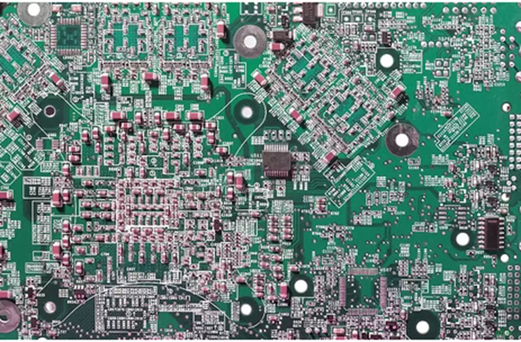
- Visual inspection
Visual inspection is one of the most basic inspection methods, involving manual observation of the appearance of the PCB circuit board, including solder joints, component mounting positions, printed circuits, etc., to identify any obvious defects or errors. - Auxiliary inspection
2.1 Thermal imaging inspection
Using infrared thermal imaging technology, hotspots on the PCB board, such as short circuits, overheating, or cold soldering issues, can be quickly detected, helping to identify potential faults early.
2.2 Infrared Transparency Inspection
Infrared transparency technology allows observation of the internal structure of the PCB board to detect any defects or abnormal phenomena, aiding in the early prevention of potential issues.
- Mechanical Inspection
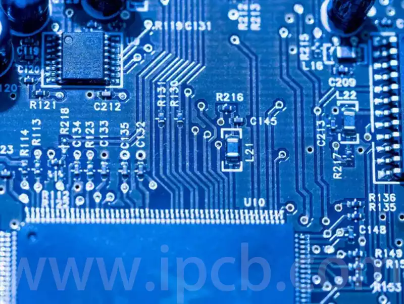
3.1 High-Magnification Microscope Inspection
Using a high-magnification microscope to conduct a detailed inspection of the PCB circuit board can identify minor soldering issues, damage, or defects, ensuring the quality of the PCB circuit board.
3.2 Visual Inspection System
An automated visual inspection system efficiently scans the entire PCB, identifying and recording any abnormalities or defects, thereby significantly improving inspection efficiency and accuracy. This system uses optical imaging principles to capture images of the PCB via a camera and compare them with standard images for analysis.
- Electrical Testing
4.1 Electrical Connectivity Testing: Electrical connectivity testing involves using a multimeter or professional electrical testing instruments to verify the connectivity between components on a PCB circuit board, ensuring that the circuit connections are correct and error-free. This method includes testing electrical characteristics such as breakdown voltage, withstand voltage, dielectric constant, and electromigration.
4.2 Component Power Consumption Testing: By measuring the power consumption of components, their normal operating status can be assessed to detect issues such as leakage, short circuits, or other electrical problems. Infrared thermal imaging cameras can be widely applied to inspect PCB circuit boards, significantly improving engineers’ efficiency by identifying thermal defects.
- X-ray Inspection
X-ray inspection clearly displays the solder joint condition of BGA-packaged devices, helping to identify hidden soldering issues and ensuring soldering quality.
- Ultrasonic Testing
Ultrasonic technology is used for defect detection in PCB circuit boards, capable of identifying voids, cracks, and foreign objects within the board layers to ensure the integrity of the PCB circuit board. The Scanning Acoustic Microscope (C-SAM) can detect defects in components, materials, and various internal issues within the PCB and PCBA.
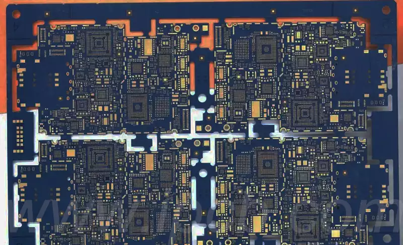
- Dimension Inspection
Dimension inspection typically uses a two-dimensional imaging measuring instrument to measure PCB boards. This instrument can accurately measure dimensions such as hole positions, length and width, and positional accuracy. Since PCBs are thin and flexible products, contact-based measurement can easily cause deformation. Therefore, non-contact imaging measuring instruments are the ideal choice for high-precision dimension measurement. Through programming, this instrument can achieve fully automatic measurement, significantly reducing measurement time and improving efficiency.
- Laser Inspection System
This represents the latest advancement in PCB testing technology. It uses a laser beam to scan the printed circuit board, collect all measurement data, and compare the actual measurement values with pre-set acceptable limit values. This technology has been validated on bare boards and is being considered for use in assembled board testing, with sufficient speed for mass production lines. Rapid output, no fixture requirements, and unobstructed visual access are its primary advantages; high initial costs, maintenance, and operational issues are its primary drawbacks.
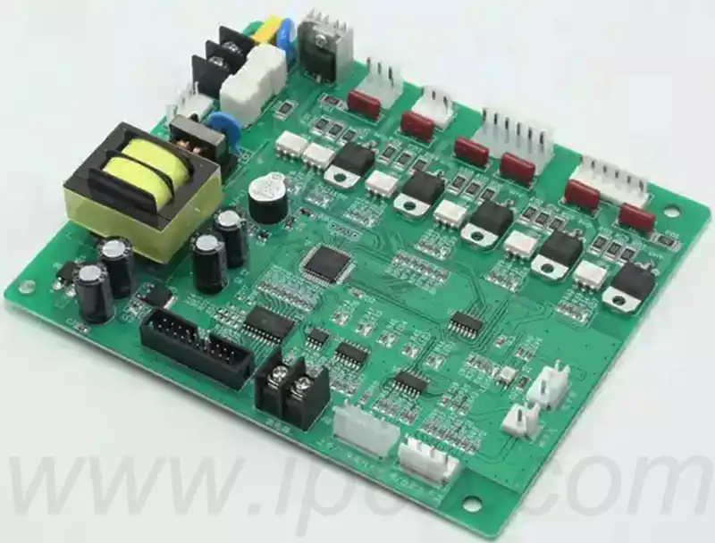
- PCB Board Functional Testing
Functional system testing involves using specialised testing equipment at the midpoint and end of the production line to conduct comprehensive testing of the functional modules of the circuit board, thereby confirming the quality of the circuit board. Functional testing can be considered the earliest form of automated testing, based on specific boards or specific units, and can be performed using various types of equipment. Types include final product testing, latest physical model testing, and stacked testing. Functional testing typically does not provide in-depth data such as component-level diagnostics for process improvement, and it requires specialised equipment and specially designed test processes. Writing functional test programs is complex, so it is not suitable for most PCB production lines.
PCB testing offers significant advantages in electronic manufacturing and quality control, ensuring the performance, reliability, and cost-effectiveness of electronic products.
- Ensuring product quality and reliability
The primary advantage of PCB testing is its ability to ensure the quality and reliability of electronic products. By conducting comprehensive testing of PCBs, defects arising during the manufacturing process—such as soldering defects, component misalignment, short circuits, and open circuits—can be identified and corrected early on. This is crucial for ensuring the optimal performance of electronic components, as even minor defects can lead to product failures, affecting the stability and lifespan of the final device. - Reducing Production Costs
PCB testing helps reduce overall production costs. By identifying and repairing defects early in the production process, defective PCBs can be prevented from entering subsequent assembly and testing stages, thereby reducing rework, scrap, and product recall costs. For example, the primary advantage of ICT (In-Circuit Testing) is its low testing cost per board, and testing programs can be generated quickly directly from CAD data without the need for special fixtures, significantly reducing testing costs. - Improving Inspection Efficiency and Accuracy
Compared to traditional manual visual inspections, modern PCB inspection technologies, especially automated inspection methods, significantly enhance inspection efficiency and accuracy.
Automated inspection: Automated technologies such as AOI (automated optical inspection) and X-ray inspection can quickly and accurately scan the entire PCB circuit board, identifying and recording any anomalies or defects. They can detect minute defects that are difficult to detect with the naked eye, reduce human error, and achieve high-precision inspection.
High Defect Coverage: Many advanced inspection methods, such as ICT, offer high defect coverage, enabling rapid and thorough testing for short circuits and open circuits, effectively detecting most potential defects.
Adapting to Complex Components and Miniaturisation Trends: As component assembly becomes more complex, circuits become more miniaturised, and Surface Mount Technology (SMT) becomes more widespread, the limitations of traditional inspection methods become increasingly evident. X-ray inspection equipment has unique advantages, capable of handling high-difficulty inspections, penetrating PCB boards to detect blind vias and other process defects—something traditional visual inspection cannot achieve.
- Enhancing production efficiency and capacity
Automated and efficient PCB inspection processes can shorten production cycles and increase overall production line throughput. The ability to quickly generate test procedures and the absence of special fixtures make the inspection process smoother, thereby improving production efficiency. For example, X-ray inspection can easily inspect internal layers from the top of the circuit, enhancing inspection efficiency. - Support for detecting complex and hidden defects
Modern PCB inspection technologies, particularly X-ray inspection and ultrasonic inspection, can detect complex and hidden defects that traditional methods cannot reach.
X-ray inspection: X-rays are non-invasive and non-destructive, enabling inspection of hidden parts of the circuit board, such as internal layers, solder joints, and defects inside vias, as well as detecting process issues like blind vias.
Ultrasonic inspection: Ultrasonic technology can be applied to PCB board inspection to detect voids, cracks, and foreign objects within the board layers, ensuring the integrity of the PCB board.
- Data Support and Traceability
Automated inspection systems typically generate detailed inspection reports and data, which are crucial for quality control, process improvement, and defect traceability. This data can be used to analyse defect patterns, optimise production processes, and provide references for future product design. - Enhancing Corporate Competitiveness
By consistently delivering high-quality electronic products, companies can enhance their market reputation and customer satisfaction, thereby strengthening their market competitiveness. High-quality PCB inspection is a critical step in achieving this goal.
Effective PCB board inspection is an important step in ensuring the quality and performance of electronic devices. By comprehensively applying various methods such as visual inspection, manual inspection, mechanical testing, electrical testing, X-ray testing, and ultrasonic testing, the quality of PCB boards can be comprehensively assessed, potential issues can be identified early, and appropriate measures can be taken to address them, thereby ensuring the normal operation of the circuit boards.