PCB components are extensively used in the PCB circuit of electronic devices. The advantage of PCB components lies in their small packaging size and the ability to meet the requirements of actual space. Except for differences in impedance value, current carrying capacity, and other similar physical characteristics, the other performance characteristics of through-hole connectors and surface mount devices are basically the same.
What does PCB component mean?
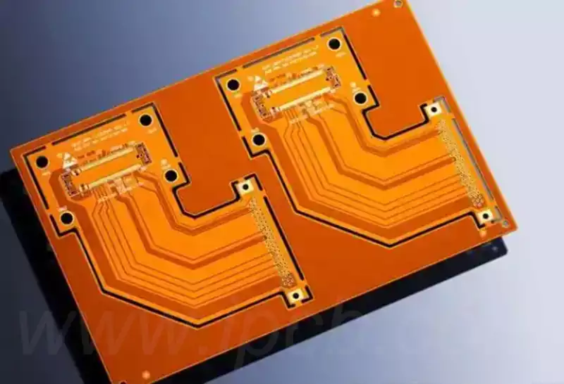
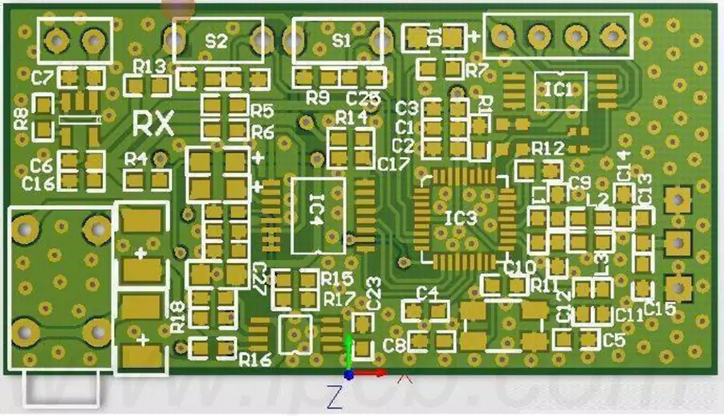
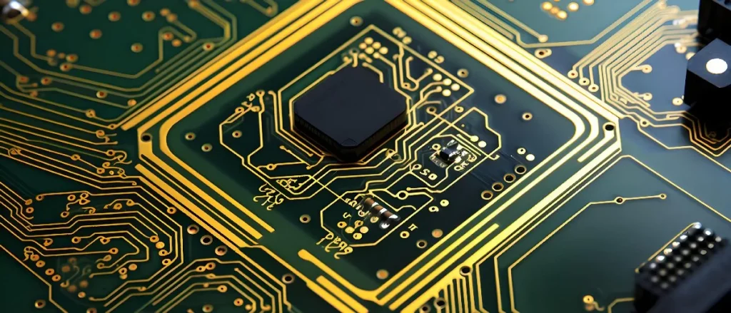
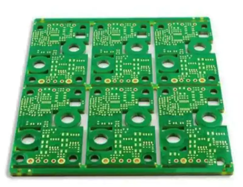
PCB components refer to various electronic components and their connecting parts on a printed circuit board, which together form a complete circuit system. PCB (Printed Circuit Board) is the core component of electronic devices, providing support and electrical connections for various electronic components. PCB enables electronic components to work in a predetermined manner through precise circuit design, achieving circuit connections and signal transmission. PCB components include but are not limited to resistors, capacitors, inductors, transistors, integrated circuits, etc. These components are fixed on the PCB by soldering or plugging, and are electrically connected to each other through wires on the PCB.
PCB components are divided into:
The main characteristics of active devices are: (1) self consumption of electrical energy, and (2) the need for external power supply.
Discrete devices, divided into (1) bipolar transistor (2) field-effect transistor (3) thyristor (4) semiconductor resistor capacitor
Analog integrated circuits mainly refer to integrated circuits composed of capacitors, resistors, transistors, etc., which are used to process analog signals. There are many analog integrated circuits, such as integrated operational amplifiers, comparators, logarithmic and exponential amplifiers, analog multipliers (dividers), phase-locked loops, power management chips, etc. The main components of analog integrated circuits include amplifiers, filters, feedback circuits, reference source circuits, switched capacitor circuits, etc. Analog integrated circuit design is mainly achieved through manual circuit debugging and simulation by experienced designers, while digital integrated circuit design is mostly automatically synthesized using hardware description languages under the control of EDA software.
Digital integrated circuit is a digital logic circuit or system made by integrating components and connections on the same semiconductor chip. According to the number of gate circuits, elements, and devices contained in digital integrated circuits, digital integrated circuits can be divided into small-scale integration (SSI) circuits, medium scale integration (MSI) circuits, large-scale integration (LSI) circuits, ultra large scale integration (VLSI) circuits, and ultra large scale integration (ULSI) circuits. Small scale integrated circuits contain no more than 10 gate circuits or no more than 100 components; Medium scale integrated circuits contain between 10 and 100 gate circuits, or between 100 and 1000 components; Large scale integrated circuits contain more than 100 gate circuits or between 10 and 10 components; The ultra large scale integrated circuit contains more than 10000 gate circuits or between 10 and 10 components; The number of components in ultra large scale integrated circuits is between 10 and 10. It includes: basic logic gates, flip flops, registers, decoders, drivers, counters, shaping circuits, programmable logic devices, microprocessors, microcontrollers, DSPs, etc.
PCB components are components that use printed circuit boards as mounting substrates to install electronic and electromechanical components, devices, or other PCB components, and achieve electrical interconnection through the PCB on the board (which can also be made into passive electronic components such as resistors, capacitors, inductors, etc.). In small electronic devices such as electronic watches, single board microprocessors, and small semiconductor radios, all components and devices are mounted on a single PCB. Large equipment, such as large computers, consists of plugins and corresponding PCB components made up of tens to thousands of PCBs. Each PCB component is usually a functional unit.
Early electronic devices, electronic and electromechanical components, and devices were mounted on a chassis made of thin metal sheets and electrically interconnected using wires. After World War II, with the development of PCB technology, electronic devices, especially electronic computers, gradually formed a structural system based on PCB components. Its advantages are good electrical performance, high reliability, small size, low cost, and the ability to achieve automated production.
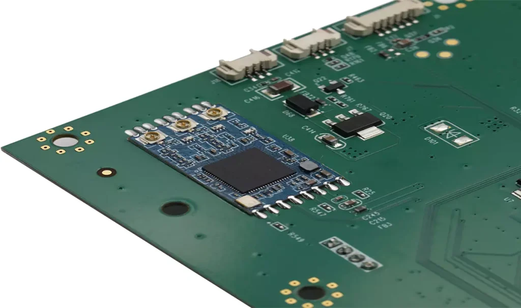
PCB components belong to the second and third level assembly.
Flat assembly or two-dimensional assembly: Components and parts are installed on a flat surface and interconnected using PCB boards. In order to increase assembly density, components and devices can be installed on both sides of the printed circuit board, or a layer of metal plate can be sandwiched between the printed circuit board to improve cooling capacity.
Modular assembly or 3D assembly: In order to increase assembly density, two parallel PCB circuit board components are generally used to form a space, and components and devices are installed in the space, or on the front and back sides of the PCB. The PCB boards are interconnected by cables or connectors; It can also be like a bridge, with the legs of components and devices placed on two printed circuit boards, called a sandwich module. The design of PCB component structure must consider issues such as circuit zoning and standardization, assembly type, reasonable layout of components and devices, assembly structure, cooling method, mechanical dynamic characteristics, etc.
Circuit zoning and standardization are reasonably divided on the system diagram, and the number of circuits, components, and devices installed on a PCB is specified. This is the circuit zoning. Simple electronic devices do not have this problem, which can be solved with just one or a few PCBs. However, in complex electronic devices such as large computers, the components of the central processing unit alone can reach over 100000 pieces. Choosing the optimal zoning plan is a complex design task. The design must first meet the requirements for electrical performance, including functionality and testability, wiring length and complexity, electromagnetic compatibility, fault location performance, and maintainability. Next is the number of external leads and its optimization. Integrated circuits have developed to large-scale and ultra large scale integration, and the number of external leads on PCBs has increased sharply, severely limiting the improvement of PCB assembly density and the full potential of large-scale integrated circuits.
The assembly of PCB components, from component and device preparation to component inspection, has been mechanized and automated. The equipment for PCB component assembly includes aging and automatic detection and classification of components and devices, equipment for shaping, cleaning, and tinning of component and device leads, automatic insertion machines for components and devices, automatic and semi-automatic winding machines, and various automatic soldering equipment. Electronic components and devices are generally installed in a plug-in manner. To improve assembly density, directly assemble with chips or chip carriers.
