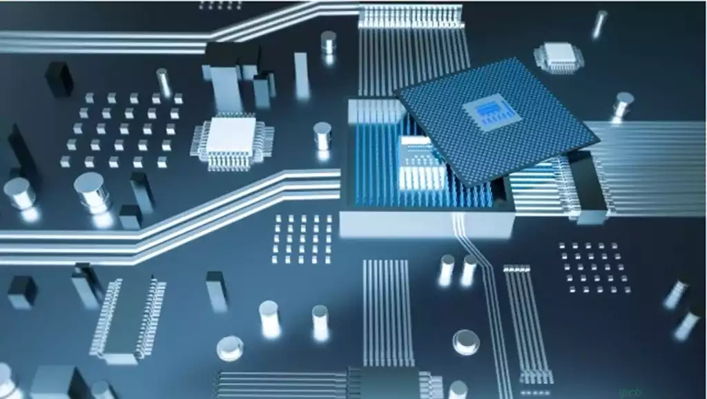
PCB layer means copper layer, PCB is made of copper layer + substrate compression and become, in addition to a single panel is a layer of copper, double-sided above the board are even number of layers. Components are soldered on the outermost layer, the other layers play a role in wire connection, but now there are some high-end PCB will be components buried inside the inner layer of the PCB.
To determine the number of layers of the circuit board (PCB), you can identify the following methods:
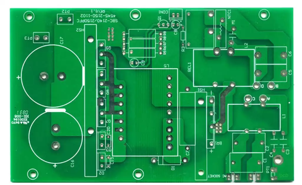
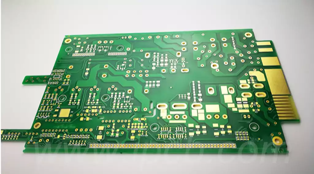
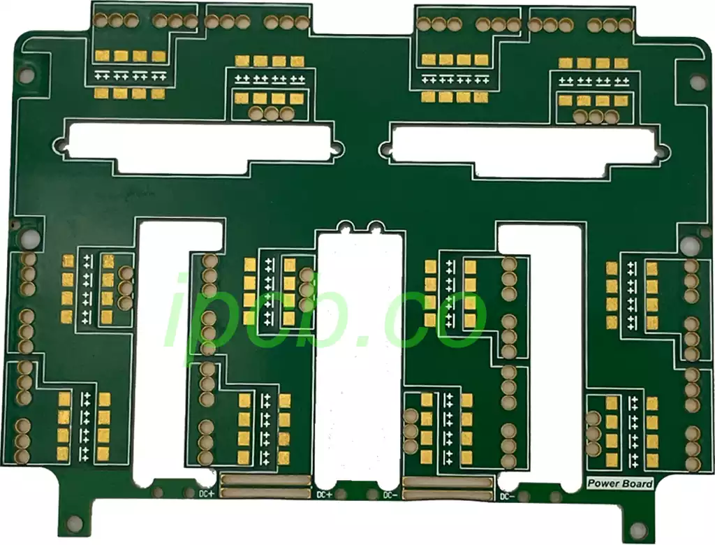
- Check the edges: Observe the edges of the circuit board. If you can see several different layers of copper cladding or sheets stacked on top of each other, then it is probably a multi-layer PCB. each copper cladding represents a separate PCB layer.
- Number of Holes: Multilayer PCBs usually have more connection holes. Look at the soldering holes on the surface and bottom of the PCB, if there are many spaced holes, then it is probably a multilayer PCB.
- Soldermask color: Different layers of a multilayer PCB are usually distinguished by different colors of soldermask. Check the surface of the PCB to see if there are areas of different colors, which may indicate differences between layers.
- Printed markings: PCB manufacturers usually mark the number of layers on the PCB substrate. Check the circuit board for printed markings or labels that may show the number of layers on the PCB.
- Through the light source: If you have a light source, try to shine the PCB substrate in a transparent way, you may be able to see the layout of the internal layers through the PCB and deduce the number of layers of the PCB.
When designing the layers of a circuit board, you should consider the following issues:
- Purpose
PCBs are used in all types of simple to complex electronic devices. Therefore, the first step is to find out whether the application has minimal or complex functionality. - The type of signal required
The choice of layers also depends on the type of signals they need to transmit, signals are categorized as high frequency, low frequency, ground or power, for applications that require multi-signal processing, multi-layer PCBs are required, these circuits may require different grounding and isolation. - Through-hole type
The choice of through-hole is another important factor to be considered. If buried through-holes are chosen, more internal layers may be required, so that multilayer requirements can be met accordingly. - Density and number of signal layers required
The determination of PCB layers is also based on two important factors: the signal layer and the pin density. the number of layers in the PCB increases as the pin density decreases. A pin density of 1.0. e.g. a pin density of 1 would require 2 signal layers. However, a pin density <0.2 may require 10 or more layers. - Number of planes required
The power and ground planes in the printed circuit board help in reducing EMI as well as shielding the signal layers. Therefore, the choice of layers will again depend on the number of planes required. - Manufacturing Cost
Though it is the main requirement, it is one of the deciding factors in selecting the number of layers in a 1-40 layer PCB design.The cost of PCB manufacturing depends on the multiple layers. Multi-layer PCBs are more expensive than single layer PCBs and the manufacturing cost will depend largely on the above requirements. - Delivery Time
The lead time of a 1-40 layer PCB based design depends on all the above factors. For example, if your design requires a single layer, the lead time may be less. If you are ordering a PCB for a complex industrial electronic device, the lead time will increase.
Often PCB designers will judge the complexity of the design circuit schematic to design by how many layers of boards, mainly from the core devices in the schematic out of the line as well as the difficulty of the apparatus layout.
In the field of electronic design, the choice of PCB layer is not simply the pursuit of high-end technology, but is the result of comprehensive consideration of performance requirements, cost budget, manufacturing feasibility and delivery time and other factors. From a simple single panel to a complex multilayer board, each step of the leap represents the progress of technology and design. Behind this are countless engineers’ pursuit of details and dedication to perfection.