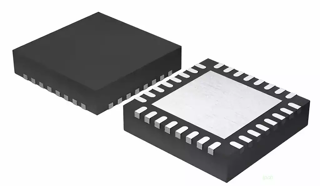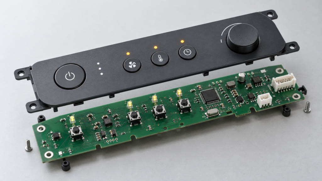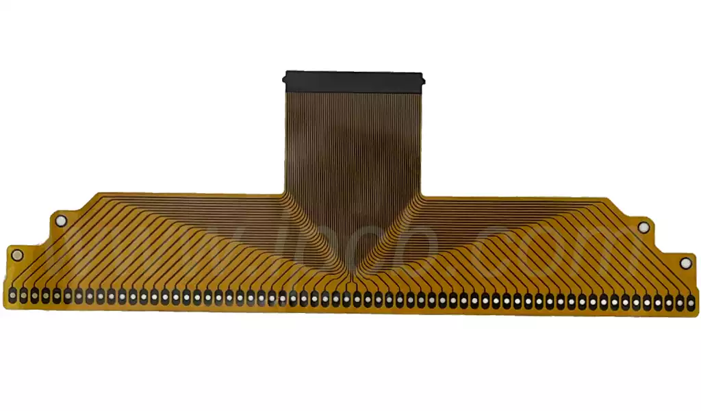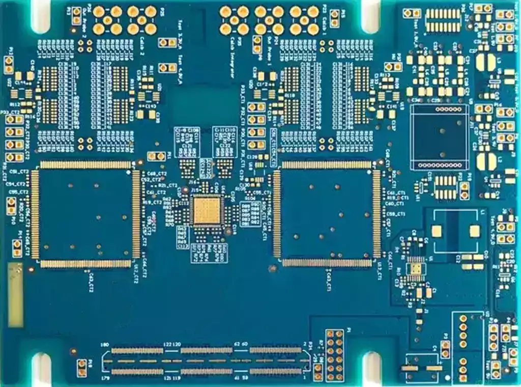
PCB replication is the process of reproducing a printed circuit board by analyzing an existing board and recovering the information needed to manufacture a replacement. It is particularly useful when original design files are missing, a legacy electronic product needs continued support, or an existing circuit board must be reproduced for authorized maintenance and development.
The process involves more than matching the board’s external dimensions. Engineers may need to identify components, reconstruct copper connections, determine the layer stackup, verify footprints, and establish suitable manufacturing specifications. For assembled boards, component sourcing, soldering requirements, and functional testing may also need to be addressed.
A successful PCB replication project should produce a board that meets defined electrical, mechanical, and manufacturing requirements. Visual similarity alone is not enough, because hidden routing, component characteristics, and subtle differences in construction can affect how the circuit performs.
When Is PCB replication Necessary?
One common reason for PCB replication is the maintenance of discontinued electronic equipment. Industrial controllers, communication devices, monitoring systems, and specialized instruments may remain in service long after their original circuit board designs become difficult to obtain. Reconstructing the necessary manufacturing information can help support replacement production and equipment maintenance.
Another situation arises when a company has a working board but cannot locate the original Gerber files, schematic, bill of materials, or assembly documentation. Recovering these details can make it easier to manufacture additional boards, investigate failures, or prepare a revised design.
Replication may also support engineering evaluation and authorized product development. Examining an existing board can reveal its component arrangement, circuit connections, layer structure, and physical interfaces. These findings can provide a foundation for understanding how the design works and deciding whether a direct replacement or an independently developed revision is more appropriate.
The required scope depends on the objective. A project intended only to replace a damaged board may need a different set of deliverables from one intended to recover a complete schematic and editable PCB layout. Defining the goal at the beginning helps establish the necessary analysis, documentation, testing, and acceptance criteria.
How the PCB Replication Process Works
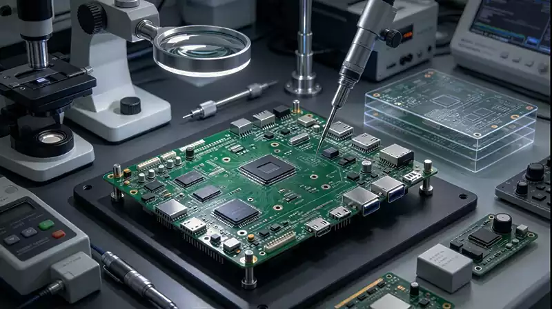
The first step is to inspect the reference board and collect all available information. Engineers record its dimensions, mounting holes, connector positions, component markings, visible copper features, and overall construction. Existing product manuals, component datasheets, photographs, and previous manufacturing records can help resolve uncertainties before more detailed analysis begins.
Next, the circuit connections and circuit board structure are investigated. For a simple single-sided or double-sided PCB, visual inspection, continuity measurements, and signal tracing may reveal much of the routing. Multilayer boards are more challenging because their internal copper layers cannot be fully inspected from the exterior. Depending on the board’s construction and required accuracy, X-ray imaging, computed tomography, or controlled destructive layer analysis may be considered.
Once sufficient information has been collected, the design data can be reconstructed. This may include a schematic, netlist, component footprints, board outline, copper routing, via locations, and layer stackup. Component identification is particularly important when markings are incomplete or obsolete parts are involved. An incorrect component value or pin mapping can change circuit behavior even when the replacement board looks almost identical to the original.
The recovered design should then undergo engineering review. Design rule checks can identify problems such as insufficient clearances, incorrect footprints, or manufacturing features outside the selected process capabilities. However, passing a design rule check does not prove that the reconstructed circuit is electrically correct. The connectivity and critical component details must be checked against the available evidence.
A prototype is usually the next important step when a complete replacement design is required. The fabricated board can be inspected for dimensional accuracy, layer construction, and electrical continuity. If components are installed, the assembled board should be evaluated against the intended operating requirements before repeat production is approved.
Technical Challenges That Affect PCB Replication Accuracy
The difficulty of PCB replication depends heavily on board complexity. A straightforward two-layer board with clearly marked components may be relatively easy to reconstruct. A dense multilayer design containing fine-pitch packages, buried connections, controlled-impedance traces, or specialized materials requires substantially more analysis.
Internal routing is one of the main challenges. Connections between components may pass through several copper layers and vias, making it difficult to establish the complete netlist through visual inspection alone. Incomplete reconstruction can result in open circuits, incorrect connections, or unexpected interactions between circuit sections.
Component identification presents another challenge. Some devices use abbreviated markings, while others may be discontinued or available in several electrically different versions. A replacement should be evaluated using its electrical characteristics, pin configuration, package, thermal requirements, and availability rather than appearance alone.
The physical construction must also be considered. Layer count, dielectric thickness, copper weight, via structure, and board thickness can affect electrical performance and mechanical compatibility. For high-speed or RF circuits, trace geometry and dielectric properties may influence impedance, insertion loss, and signal integrity. Reproducing only the visible routing without recovering these requirements may lead to a board that passes basic continuity checks but fails in operation.
A further challenge is distinguishing confirmed information from assumptions. If a buried connection cannot be verified or a component’s exact specification remains uncertain, that limitation should be documented. Recording unresolved questions makes it easier to plan additional inspection or testing rather than treating an estimated design detail as a verified fact.
Manufacturing and Testing the Reconstructed Board
After design recovery, manufacturing specifications should be established before the replacement PCB enters production. The package may include Gerber or ODB++ files, NC drill data, a layer stackup, material requirements, board dimensions, copper specifications, surface finish, and any controlled-impedance requirements. If assembly is included, the bill of materials, placement data, assembly drawings, and testing instructions should also be defined.
Manufacturing controls help ensure that the reconstructed design can be reproduced consistently. The board outline and mounting features must match the product’s mechanical interfaces, while conductor geometry and layer registration must meet the electrical requirements. Specialized materials or unusual via structures may require additional review to confirm that the selected fabrication process can achieve the intended result.
Testing should reflect the purpose of the replication project. Bare-board electrical testing can identify certain manufacturing defects, but it cannot confirm that the complete circuit performs its intended function. For assembled boards, inspection may include automated optical inspection, X-ray inspection for suitable hidden-joint packages, and checks for soldering defects.
Functional testing is especially important when the original board controls equipment or communicates with other systems. Power-up checks, voltage measurements, interface verification, firmware compatibility, and application-specific tests can help establish whether the replacement behaves as expected. High-speed, RF, power, or safety-critical designs may require additional measurements or qualification procedures.
Before approving repeat production, the team should compare prototype results against the agreed requirements. Any component substitutions, design changes, or unresolved deviations should be documented. This creates a more dependable manufacturing baseline than relying solely on a physical reference board.
PCB Replication and Long-Term Design Control
Reproducing a board once does not automatically create a sustainable replacement process. For ongoing production, the recovered files should be organized into a controlled design package that identifies the approved revision, component specifications, manufacturing requirements, assembly instructions, and test criteria.
This documentation is particularly valuable when components become obsolete or suppliers change. A controlled process allows engineers to assess proposed substitutions and determine whether they affect circuit behavior, thermal performance, electrical characteristics, or mechanical fit. Changes should be verified before they are incorporated into a production release.
Intellectual property must also be considered before work begins. PCB replication may be appropriate for authorized repair, maintenance, or recovery of a company’s own design, but the right to inspect a physical board does not automatically grant permission to reproduce or commercially distribute every protected design. Patents, contractual restrictions, trade secrets, copyright, and jurisdiction-specific rules may affect what can legally be done. The project’s authorization and intended use should therefore be clarified in advance.
Ultimately, PCB replication is most effective when it combines careful physical inspection, accurate circuit reconstruction, appropriate manufacturing specifications, and functional verification. By treating the reference board as engineering evidence rather than a picture to copy, teams can develop replacement circuit boards that are more consistent, maintainable, and suitable for their intended application.