Silkscreen printing is typically employed to mark useful information on PCB boards, aiding users during the assembly process. It serves to label component values, part numbers, polarity, and other details, while also incorporating version numbers, manufacturer information, and similar data. PCB silkscreen printing is completed during the PCB manufacturing process, yet it is utilised in PCB assembly steps. The silkscreen can consist of letters, numbers, or text.
Typically, PCB silkscreen printing employs white ink, a common colour chosen for its manufacturing compatibility. Additionally, other colours such as yellow, red, and black are frequently used during the initial stages of PCB board design. Pink silkscreen is favoured by some PCB layout designers, though its use is generally discouraged due to its specific characteristics that render it less suitable for the manufacturing process.
The primary functions and characteristics of the silkscreen layer include:
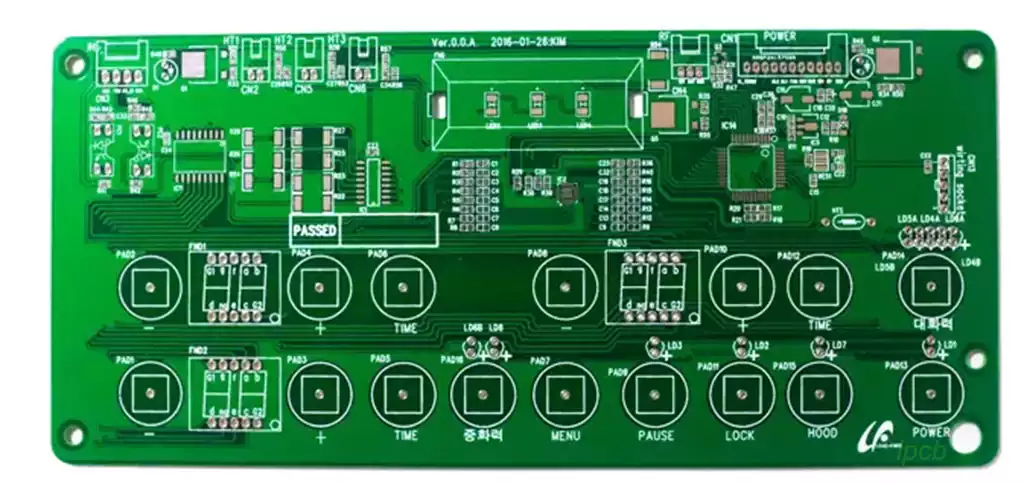
- Annotation and Marking: The silkscreen layer typically bears component part numbers and nominal values, component outline shapes, manufacturer logos, production dates, and various annotation characters. These include component projection outlines, component labels, nominal values, or model designations. Such information is crucial for circuit installation, debugging, maintenance, and production management.
- Production Facilitation: Printing component outlines, serial numbers, and other explanatory text onto the component side or solder side via screen printing significantly aids insertion operations (including surface-mount component placement) during PCB manufacturing.
- Layout Principles: Character placement on the silkscreen layer must adhere to the principles of ‘unambiguous presentation, efficient use of available space, and aesthetic appeal’ to ensure information accuracy and readability.
Position and Function of the Silk Screen Layer in PCB Design:
The silk screen layer resides on the topmost layer of the PCB (or occasionally the bottom layer), functioning as either the top or bottom layer in the design.
It is not part of the actual circuit routing layer but serves to provide supplementary information and annotations, aiding engineers and technicians in better understanding and handling the circuit board.
Complete Process of PCB Silkscreen Printing
- Designing the Silk Screen
Design the silk screen layer using EDA software. This includes identifying and assembling all necessary markings, symbols, and text required for component placement on the PCB. Export the design in a format compatible with the manufacturer’s equipment. - PCB Manufacturing
The PCB fabrication process involves printing a layer of copper onto the substrate, drilling holes for components, then etching away excess copper to create the PCB, which may feature various shapes and patterns. A specialised screen printing process is employed to apply the silkscreen layer atop the copper layer. - Application of Silkscreen Printing
Upon PCB fabrication completion, the silkscreen layer is printed using the screen printing process. This involves creating a stencil for the silkscreen design. The stencil is formed by applying photosensitive emulsion to the mesh to create the desired image pattern. - Curing the Ink
After applying the screen-printed layer, the ink must be cured to ensure proper adhesion to the PCB substrate. This is typically achieved by exposing the PCB to high temperatures or ultraviolet light for a specified duration. - Inspection and Testing of the PCB
The PCB undergoes final inspection and testing to verify that the screen-printed layer has been applied correctly and that all required markings and symbols are present. Errors or omissions in screen printing can lead to assembly faults or functional issues.
Considerations for PCB Screen Printing Design:
To ensure all letters, numbers, and symbols are readily identifiable on the PCB, screen printing line widths must exceed 5 mil, with a minimum height of 50 mil.
Screen printing must not overlap with pads or reference points.
White is the default screen printing ink colour. Any special requirements must be specified in the PCB drill file.
In high-density PCB designs, silkscreen content may be selected as required. Silkscreen character strings are arranged left-to-right and bottom-to-top.
What specific requirements apply to component silkscreen design?
All components, mounting holes, locating holes, and locating/identification points must bear corresponding silkscreen markings, positioned clearly and unambiguously.
For components on the PCB with polarity or directional mounting requirements, both polarity and orientation must be indicated via silkscreen.
The minimum clearance between silkscreen markings and soldering areas (e.g., SMT pads, through-hole mounting holes, test points, reference points) shall be 0.4mm.
To facilitate inspection, silkscreen characters, polarity indicators, and directional markings must not be obscured by components, pull tabs, or similar elements.
Where space constraints necessitate omitting silkscreen symbols for certain components on the PCB, these symbols must be retained on the PCB assembly drawing. Components shall be positioned via the assembly drawing.
What are the key considerations for pcb silkscreen design?
To ensure reliable component soldering, no silkscreen shall be applied over component pads (i.e., silkscreen must not overlay pads).
To facilitate component insertion and maintenance, component part numbers must not be obscured by installed components.
Silkscreen printing must not overlay vias or pads, as this may cause partial loss during solder mask opening, impairing identification.
Polarity of polarised components must be clearly marked on the silkscreen diagram, with polarity direction indicators easily discernible.
Directionality of directional connectors must be clearly indicated on the silkscreen.
PCB silkscreen printing design, as an indispensable element in circuit board manufacturing, not only fulfils crucial functions such as component identification and assembly guidance but also directly impacts the board’s manufacturability. By adhering to scientific design principles, rigorous manufacturing processes, and meticulous precautions, we can ensure the accuracy and legibility of silkscreen information, thereby providing robust support for subsequent assembly, testing, and maintenance operations.