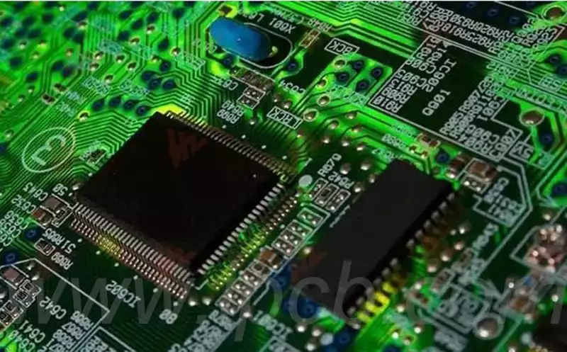
Printed Circuit Boards are critical components in the electronics manufacturing world and PCB stencil, as a core tool in the PCB manufacturing process, are of paramount importance.
What is a stencil?
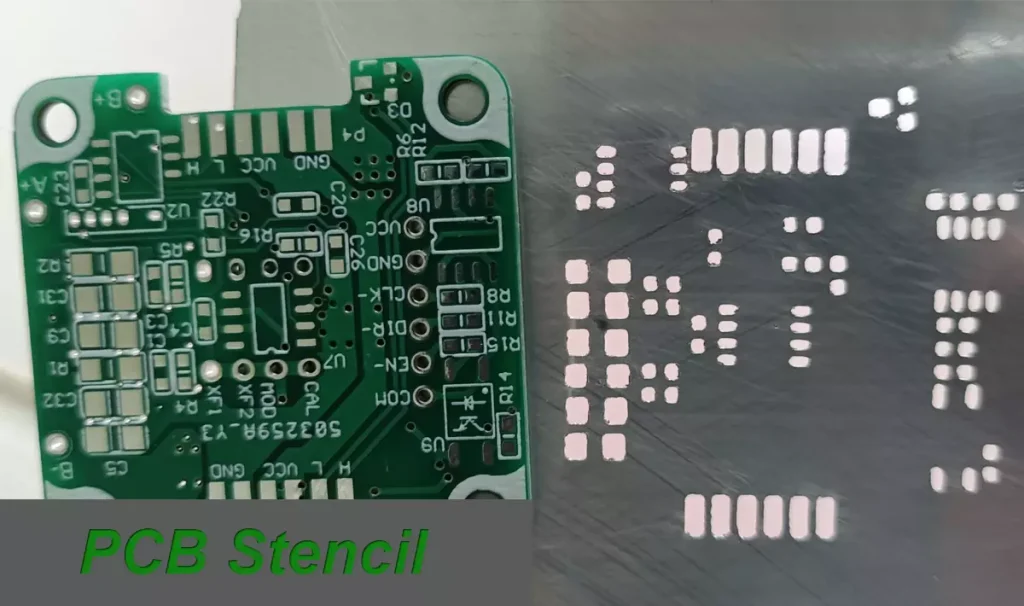
A PCB stencil, as the name suggests, is a mesh structure made of metal that is used to carry and transfer ink during the printed circuit board manufacturing process. During the circuit board printing process, the stencil acts as a template to ensure that the ink is applied exactly where it is intended to be on the PCB board, forming fine lines.
PCB Stencil Advantages
High precision: The high precision and stability of stencil material ensure the accuracy and consistency of printed circuits, thus improving the quality and reliability of circuit boards.
Efficient production: Printing with PCB stencils enables fast and continuous production, increasing productivity and reducing production costs.
Environmentally sustainable: Stencils have a long service life and can be reused to reduce waste, meeting the requirements of environmental sustainability.
PCB Stencil Classification1、
1. Classified by PCB material
Stainless steel stencil: stainless steel is a metal material with high strength, corrosion resistance, and good electrical conductivity. Stainless steel stencils are widely used in the manufacturing process of printed circuit boards because of their high precision, high stability, long life, and other advantages.
Nickel stencil: nickel has good electrical conductivity, corrosion resistance, and abrasion resistance, so nickel stencils are favored in some special applications, such as the manufacture of electronic devices in a high vacuum environment.
2. According to the aperture classification
Standard Aperture Stencil: The aperture specifications of standard Aperture stencil follow certain industry standards and apply to the manufacturing of general printed circuit board.
Non-standard aperture PCB stencil: The aperture specification of non-standard aperture PCB stencil can be customized according to the customer’s demand, which applies to the manufacturing of printed circuit boards with special sizes or high precision requirements.
3. Classification by application
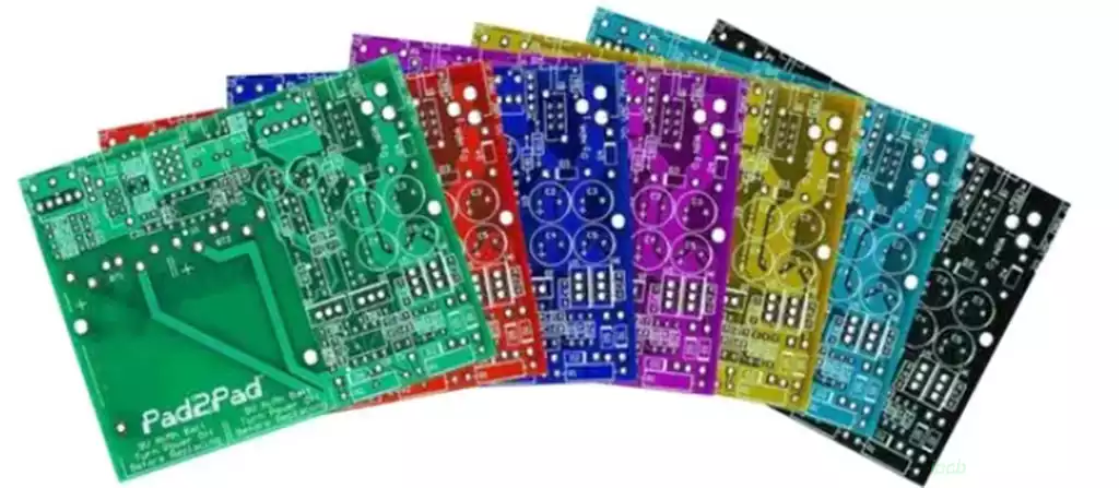
Single-panel PCB stencil: Single-panel PCB stencils are suitable for the manufacture of single-sided printed circuit boards, with a relatively simple structure, usually with only one layer of metal mesh.
Double-sided PCB stencil: double-sided PCB stencil for double-sided printed circuit board manufacturing, its structure is relatively complex, with two different layers of metal mesh, can realize the circuit in the two sides of the printing.
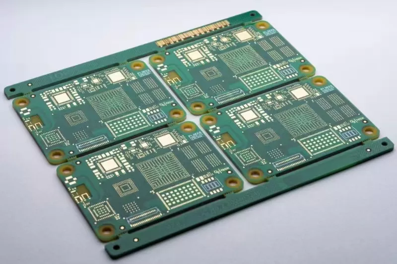
Multi-layer PCB stencil: Multi-layer PCB stencils are suitable for the manufacture of multi-layer printed circuit boards, whose structure consists of multiple conductive and insulating layers, and the manufacturing process is more complex.
4. Classification according to precision
Ordinary precision PCB stencils: The printing line precision of ordinary precision PCB stencils is within a certain range, which is suitable for the manufacturing of printed circuit boards with low precision requirements.
High-precision PCB stencil: high-precision PCB stencil printing line precision, can reach a micron or even nanometer level, applicable to high-precision, high-reliability requirements of the printed circuit board manufacturing, such as cell phones, computers, and other electronic products in the printed circuit board.
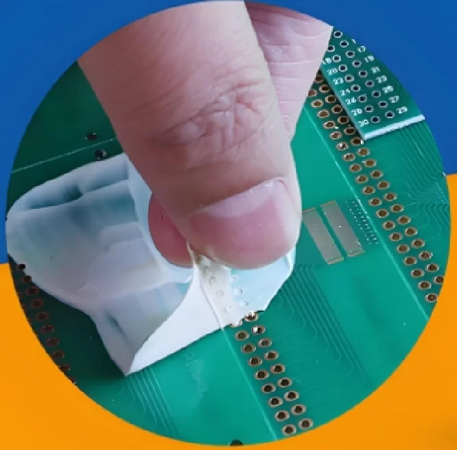
How to make a PCB stencil?
Material Preparation: Choose suitable steel as the raw material for making stencils, commonly used are common steel, stainless steel, and aluminum alloy.
Cutting: Cut the selected steel according to the size requirements, you can use manual cutting, machine cutting, and other ways.
Welding: Use electric or gas welding to weld the cut steel and fix the mesh area.
Finishing: After welding is completed, finishing work is carried out, including removing defects and burrs caused by welding, to make the whole surface of the steel mesh flat.
Drilling: Drill holes in the PCB stencil as required to get the required specification of the stencil.
Cleaning: Clean the PCB stencil to remove the impurities and dirt left on the surface to ensure its cleanliness.
Testing: Test the stencil to ensure that it meets the quality standards.
Packing: Pack the qualified PCB stencil to protect its quality and safety during transportation and storage.
How to choose the right PCB stencil?
Determine the stencil specifications: According to the size and design requirements of the printed circuit board, select the appropriate PCB stencil specifications, including frame size, mesh size mold opening size, etc.
Material Selection: Select the appropriate PCB stencil material, such as stainless steel, nickel, etc., according to the actual requirements to ensure printing quality and stability.
Precision requirements: According to the precision requirements of circuit board manufacturing, select high-precision and high-stability PCB stencils to ensure the accuracy and consistency of the line.
Quality Assurance: Choose a PCB stencil manufacturer with guaranteed quality to ensure the quality and reliability of the PCB stencil and reduce the risk in the production process.
PCB stencils are an important tool in electronics manufacturing and play a key role in realizing efficient, high-quality PCB manufacturing.