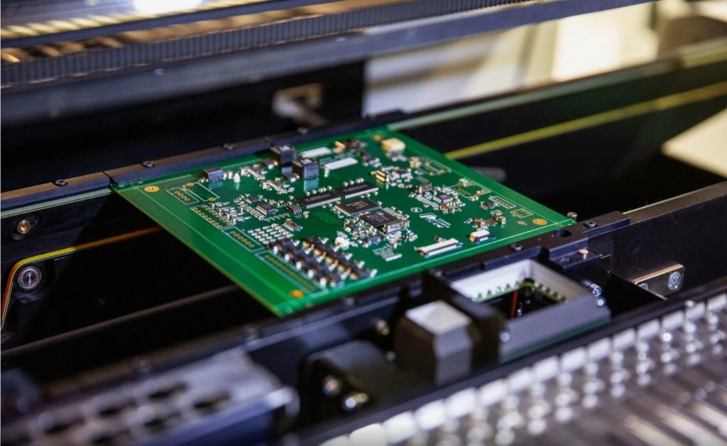
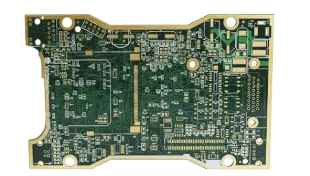
A prototype pcb fabrication is the first actual circuit board that is fabricated from circuit design drawings during the design and development of an electronic product. This prototype is used to verify the correctness, functionality and layout of the circuit design. Printed circuit board prototyping is the process of translating an electronic circuit design into an actual physical circuit board. In this process, the designer first uses electronic design automation (EDA) software to create the circuit board’s graphics and layout, and then translates this design data into an actual board that can be manufactured.
pcb prototype fabrication service is an important service in the electronic product development process,helping design teams to quickly validate design solutions, reduce development risks, and provide a foundation for subsequent product iterations.Through PCB prototyping, designers and engineers can better understand the actual performance of a circuit in order to further optimize design solutions and improve product quality.
How does a PCB prototype work?
PCB prototypes provide a central hub for integrating all electronic components in a device. For 2-layer PCB prototypes or multi-layer PCB prototypes, conductor paths or wires can be laminated to the PCB prototype substrate data. These copper wires are used as conductor circuits for all components soldered to the PCB prototype board to power the equipment while providing insulation and safe current transfer.
General steps in PCB prototyping:
Design and Drawing Production:
The designer first draws the circuit schematic using specialized electronic design automation (EDA) software.
Then, PCB design software (such as AutoCAD, EAGLE, Altium Designer, etc.) is used to draw wiring diagrams to determine the location and connection relationship of each component on the circuit board.
Material selection and preparation:
According to the requirements of the circuit design, select the appropriate substrate material (e.g. FR4, CEM-1, etc.) and copper foil thickness.
Prepare other necessary materials such as solder, flux, wires, resistors, capacitors, ICs and other electronic components.
Make the circuit board:
Transfer the designed circuit pattern to the substrate by photolithography or inkjet printing techniques.
Etches or cuts copper foil into desired circuit patterns using chemical etching or laser cutting techniques.
Performs drilling operations to provide the necessary holes for component soldering and assembly.
Soldering and Assembly:
Solder electronic components to circuit boards as required by circuit diagrams.
Connects and secures wires as required.
Testing & Verification:
Performs functional and performance tests on the circuit board using test equipment (e.g., oscilloscope, multimeter, etc.).
Verify that the board’s functions meet the design requirements.
Revision and Optimization:
Based on the test results, revise and optimize the circuit board design as necessary.
Repeat the above steps until a satisfactory design and performance is achieved.
Documentation and Delivery:
Organize all documentation and test reports from the production process.
Deliver the completed PCB prototype to the customer or for subsequent product development.
PCB prototypes are widely used because of their many advantages:
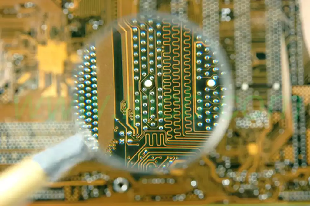
High Integration: As integrated circuits become more integrated and mounting technology advances, high density printed circuit boards are developed. This means that more electronic components can be tightly integrated into a smaller space, improving the performance of electronic devices.
High reliability: PCB prototypes can work stably for long periods of time through a series of inspection, testing and aging tests, and their service life is usually up to 10-20 years. This makes PCB prototypes a reliable choice for long-term applications.
Design Flexibility: Through design standardization and normalization, PCBs can meet a variety of requirements in electrical, physical, chemical, and mechanical aspects. This design flexibility allows PCB prototypes to have shorter development cycles and improved design efficiency.
Production efficiency: With modern management, PCB prototypes can be standardized, scaled (quantity) and automated production to ensure the stability of product quality. This improves production efficiency and reduces production costs.
Easy to test: A more complete test methodology and test standards have been established. Through a variety of test equipment and instruments, you can accurately detect and identify the qualification and service life of PCB prototype products.
Easy to assemble: PCB products facilitate the standardized assembly of various components and automated mass production. In addition, PCBs and other functions can be assembled as a whole to form more important components, systems, or even entire machines. This ease of assembly makes PCB prototypes more efficient in the manufacturing process.
Easy to maintain: Since the parts and various components assembled in a PCB product are designed and produced according to a standardized pipeline, these parts are also standardized. This means that in the event of a system failure, components can be replaced quickly, easily and flexibly, allowing the system to quickly return to normal operation.
In addition, PCB prototyping has the advantages of small size, light weight, and fast circuit transfer speed, which makes it widely used in various electronic devices.
Prototype pcb fabrication is an indispensable part of the development process of electronic products. It can not only verify the correctness and feasibility of the circuit design, but also provide strong support for the subsequent development of the product.