RF circuit board design is an important technology in the development of modern electronic equipment, widely used in wireless communications, radar, intelligent devices and other fields. Due to the unique high-frequency characteristics of RF signals, every detail of the design process will significantly affect the quality of signal transmission and the overall performance of the system.
The main factors to be considered in the RF circuit board design process:
- Impedance matching
Impedance matching is one of the core elements of RF PCB design. When the characteristic impedance of the circuit is kept consistent, maximum power transmission can be realized and signal reflection and loss can be avoided. Therefore, the design process needs to accurately calculate and design the width of the signal alignment, the dielectric constant of the PCB material, etc. to meet the specific impedance requirements. - Material Selection
The materials used in RF circuit board has a significant impact on circuit performance.The selected material should have low signal loss, stability in the high frequency range, and can effectively dissipate heat.The dielectric constant and loss angle tangent of the material should also be consistent at different frequencies to ensure high frequency signal transmission. - Layer stacking method
Reasonable layer stacking design can significantly improve the performance of RF circuits.Multilayer PCB design can effectively isolate the power supply layer and ground layer, thereby reducing electromagnetic interference and optimizing signal integrity.The number of layers of the board and its arrangement are key factors that need to be carefully considered in the design. - Component Layout
Component layout directly affects the signal transmission path and circuit interference. The placement of RF components and vias need to follow certain principles to minimize the length of the signal path and avoid cross. Attention should also be paid to the isolation between high-frequency signals and low-power signals in the layout to mitigate potential interference problems. - Signal Alignment Design
In RF circuit board design,signal alignment design is especially critical.The alignment should be as short and straight as possible to reduce transmission delay and reduce power loss.At the same time,the appropriate type of alignment should be selected, such as coplanar waveguide, microstrip line and ribbon line, in order to optimize the signal propagation characteristics. - Grounding Design
Good grounding design is the cornerstone to ensure signal quality.The grounding layer needs to be reasonably configured to ensure the shortest path for return current to reduce impedance and noise interference.At the same time,a large area of grounding should be used to increase signal integrity and reduce electromagnetic interference. - Power decoupling
Power decoupling is another important factor to ensure the stability of RF circuits. RF circuits are very sensitive to noise,so it is necessary to use appropriate decoupling measures to reduce the noise impact on the power supply. Through the power supply decoupling design, you can maintain the integrity of the power supply to ensure stable operation of the circuit.
RF Circuit Power Supply Design Considerations
The power line is an important way for EMI to enter and exit the circuit. Through the power line, outside interference can be transmitted into the internal circuit, affecting the RF circuit index.In order to reduce electromagnetic radiation and coupling, the DC-DC module is required to minimize the area of the primary side, secondary side, and load side loops. Power supply circuits,no matter how complex the form,have high current loops that are as small as possible. Power and ground wires should always be placed very close together.
If a switching power supply is used in the circuit, the peripheral device layout of the switching power supply should conform to the principle of the shortest return path for each power. Filter capacitors should be placed close to the relevant pins of the switching power supply. Use common mode inductors close to the switching power supply module.
Long power lines on a single board should not approach or pass near both the output and input of a cascade amplifier (with a gain greater than 45dB). Avoid power lines that become RF signal transmission paths, which may cause self-excitation or degrade sector isolation. High-frequency filter capacitors need to be added to both ends of long power lines, and even to the center.
RF PCB power inlet combination of parallel connection of three filter capacitors,the use of these three capacitors of their respective advantages were filtered out of the power line on the low, medium and high frequency. For example:10uf, 0.1uf, 100pf, and in accordance with the order from large to small close to the input pin of the power supply.
With the same set of power supply to the small signal cascade amplifier feed, should start from the last stage,in order to supply power to the front stage, so that the EMI generated by the circuit of the last stage of the front stage of the impact is smaller.And each level of power filtering at least two capacitors: 0.1uf, 100pf. When the signal frequency is higher than 1GHz, to increase the 10pf filter capacitance.
Commonly used in low-power electronic filters,filter capacitance to be close to the triode pin,high-frequency filter capacitance closer to the pin. Triode selection of lower cutoff frequency.If the triode in the electronic filter is a high-frequency tube,working in the amplification area,the layout of the peripheral devices and unreasonable,in the power supply output is easy to generate high-frequency oscillation.Linear voltage regulator module may also have the same problem, the reason is that there is a feedback loop within the chip,and the internal transistor works in the amplification area.In the layout of the requirements of high-frequency filter capacitors close to the pin,reduce the distribution of inductance,destroying the oscillation conditions.
The size of the copper foil of the POWER part of the PCB is in line with the maximum current flowing through it,and consider the margin (generally referenced as 1A/mm line width).
The input and output of power supply lines should not be crossed.
Pay attention to power decoupling and filtering to prevent different units from interfering through the power lines,and the power lines should be isolated from each other when power wiring.The power supply lines should be isolated from other strong interference lines (e.g. CLK) by ground lines.
The power supply wiring of small signal amplifier needs to be isolated by ground copper skin and grounding hole to avoid other EMI interference from running in, which will deteriorate the signal quality of this level.
Different power supply layers should avoid overlapping in space. Mainly to reduce the interference between different power supplies, especially some of the voltage difference between the power supply,the overlap of the power plane must try to avoid,it is difficult to avoid can be considered in the middle of the ground layer.
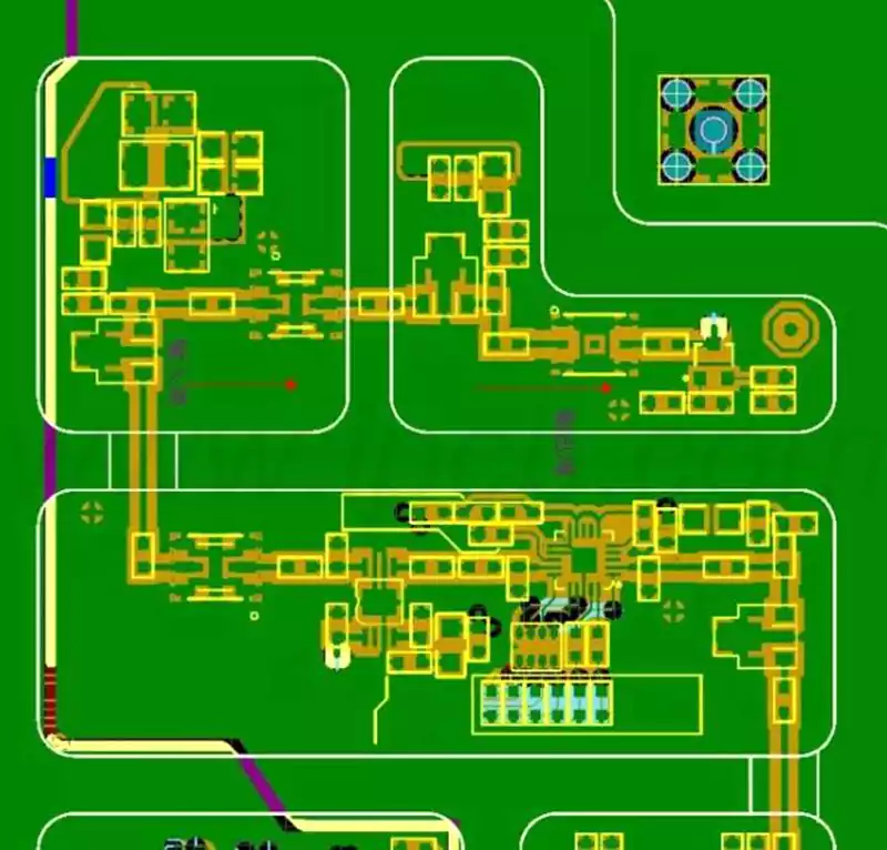
PCB board layer distribution to facilitate the simplification of subsequent wiring processing,for a four-layer PCB board (commonly used in WLAN circuit boards), in most applications with the top layer of the board to place components and RF leads,the second layer as the system ground, the power supply is placed in the third part of the third layer, any signal lines can be distributed in the fourth layer.
EMC Specifications for RF PCB Design
- Layer Distribution
In RF circuit board design, layer distribution design is crucial. Common design specifications are: for double-sided boards, the top layer is designed to be the signal layer, and the bottom surface is the ground plane; while for four-layer boards, the top layer is the signal layer, the second layer is the ground plane, and the third layer takes the power and control lines. This design helps to achieve good electromagnetic shielding and signal integrity. - Shielding and Isolation
Shielding is an important EMC requirement in RF circuit board design.Effective shielding and isolation techniques can reduce the impact of interference from external sources. Through the use of metal cases or specialized shielding materials,the electromagnetic compatibility of the circuit can be improved to prevent internal signals from being interfered by external stray signals. - Grounding design
Good grounding design can significantly improve the electromagnetic compatibility.A wide and continuous ground plane should be used to provide a low impedance return path. This helps to reduce the loop area and hence the risk of EMI. - Signal Alignment Strategy
A proper signal alignment strategy is also critical to improving EMC performance.It is necessary to ensure that RF signal lines are kept away from sources of interference and that the length of the signal alignment is kept as short as possible.In addition,the use of appropriate alignment width and spacing to maintain impedance matching can effectively improve signal integrity. - Electrostatic discharge (ESD) protection
RF circuit board design also need to consider electrostatic discharge (ESD) protection.Reasonable design measures can effectively prevent electrostatic damage to the circuit,thereby improving system reliability.This includes the use of appropriate ESD protection components and the proper design of grounding paths.
RF circuit board design is a complex process covering a wide range of technologies.By choosing the right materials, optimizing the layout,strengthening grounding and signal isolation and other measures, engineers can significantly improve the performance and stability of the circuit. Mastering these design principles will help develop more efficient and reliable electronic devices in future wireless communication technologies.