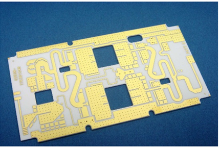
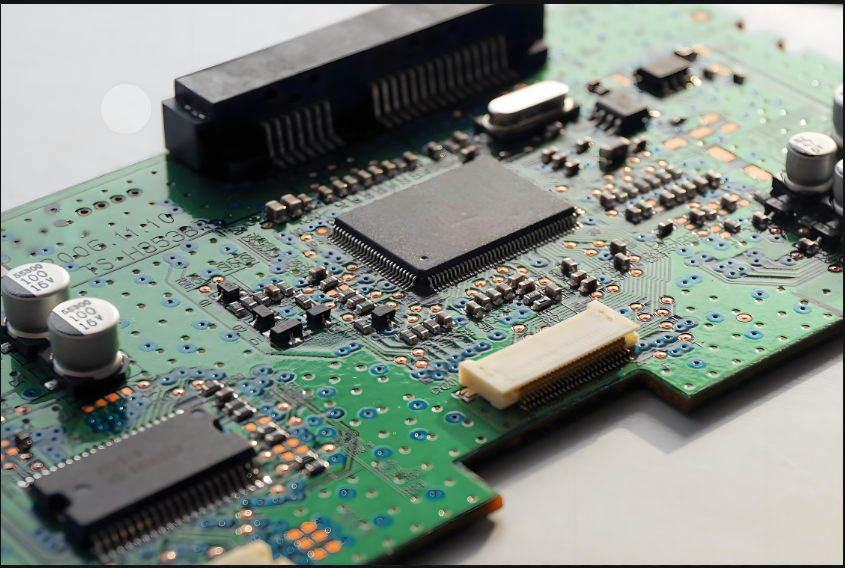
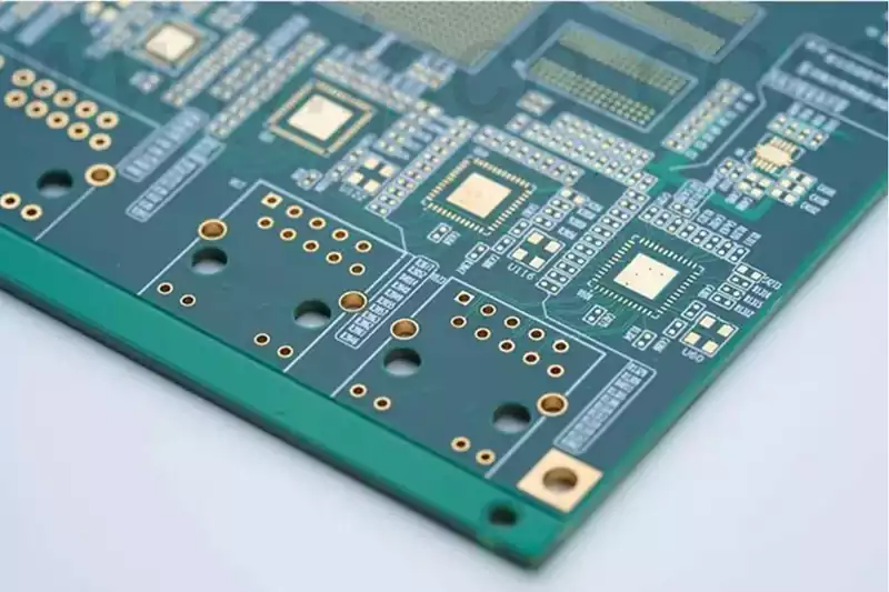
A Teflon PCB is a printed circuit board that uses polytetrafluoroethylene (PTFE) as its primary dielectric material. Compared with many conventional PCB substrates, PTFE offers a lower dielectric constant and extremely low dielectric loss, making it well suited for RF and microwave circuits where low signal loss and stable electrical performance are critical. Teflon PCBs are widely used in RF communication equipment, radar systems, antennas, satellite electronics, and other high-frequency applications.
Teflon PCBs use PTFE-based copper-clad laminates (CCLs) instead of conventional epoxy-based substrates. The dielectric material separates the conductive copper layers while controlling the electrical characteristics of the signal transmission path. Because the dielectric constant (Dk) and dissipation factor (Df) of the substrate directly affect high-frequency signal transmission, material selection is a critical part of RF and microwave PCB design.
PTFE has a relatively low dielectric constant and an extremely low dissipation factor. These properties help reduce dielectric losses as electromagnetic signals propagate through transmission lines. The actual electrical properties vary depending on the specific PTFE laminate, reinforcement system, resin content, copper foil type, operating frequency, and test method. Therefore, designers should always use the material parameters provided in the laminate manufacturer’s official datasheet rather than treating a single set of PTFE performance values as a universal standard.
Why Use Teflon PCBs for High-Frequency Circuits
Compared with low-speed signals, high-frequency signals are more sensitive to dielectric loss, conductor loss, impedance variation, copper foil surface roughness, and dimensional changes in the PCB. As frequency increases, even small variations in the transmission structure can affect insertion loss, phase characteristics, and impedance matching.
PTFE-based substrates can provide very low dielectric loss and stable electrical performance, helping reduce signal attenuation in RF and microwave transmission lines. PTFE also has very low water absorption, which helps maintain stable electrical characteristics in high-humidity environments and minimizes changes in dielectric properties caused by moisture.
Because of these characteristics, Teflon PCBs are particularly suitable for microwave circuits, antenna feed networks, RF power amplifiers, filters, power dividers, radar systems, and other high-frequency electronic products.
The final performance of a Teflon PCB is not determined by PTFE resin alone. Commercial PTFE-based copper-clad laminates are available with different reinforcement structures, ceramic fillers, and other fillers to adjust dielectric constant, dimensional stability, thermal characteristics, and manufacturing compatibility.
The dielectric constant (Dk) affects the propagation characteristics of signals within the PCB, while the dissipation factor (Df) characterizes dielectric loss. In high-frequency PCB design, these two parameters should be evaluated together with copper foil roughness, trace geometry, laminate thickness, and operating frequency.
A lower Df generally helps reduce dielectric loss, but material selection should not be based on Df alone. Engineers should also evaluate the target Dk, Dk stability over frequency, coefficient of thermal expansion (CTE), water absorption, thermal conductivity, copper peel strength, and mechanical properties.
Dielectric thickness also affects impedance. The performance of a controlled-impedance transmission line is determined by factors including trace width, copper thickness, dielectric thickness, dielectric constant, and the associated reference plane. Changing any of these parameters can alter the resulting characteristic impedance.
Teflon PCB vs. FR-4 PCB
FR-4 remains the most widely used PCB substrate because it provides a good balance of cost, mechanical strength, manufacturability, and electrical performance. It is suitable for most digital circuits, analog circuits, industrial equipment, and consumer electronics.
Teflon PCBs are typically selected when a product requires higher high-frequency electrical performance. PTFE-based copper-clad laminates can provide lower dielectric loss and more stable high-frequency electrical characteristics, but they also require specialized PCB manufacturing processes.
Substrate selection should be based on the actual requirements of the circuit rather than simply choosing the material with the lowest loss. Using PTFE for a low-frequency control circuit can increase material and manufacturing costs without providing a meaningful electrical benefit. For microwave circuits operating in the multi-GHz range, however, dielectric and conductor losses become increasingly significant, making low-loss PCB materials essential.
Teflon PCB Manufacturing Process
Teflon PCB manufacturing is generally more challenging than conventional FR-4 PCB fabrication. The unique mechanical and thermal characteristics of PTFE materials affect drilling, copper adhesion, lamination, plating, and dimensional control throughout the manufacturing process.
Compared with conventional PCB substrates, PTFE materials are relatively soft. Therefore, drilling parameters must be carefully controlled to achieve clean hole walls and minimize drilling defects. For plated through-holes (PTHs) and vias, hole-wall quality is particularly important because the metallized structure must provide reliable electrical connections between copper layers.
Copper adhesion is another critical consideration. PTFE has a highly chemically inert surface, so the interface between the copper foil and dielectric material requires specialized surface treatment and strict process control. The specific treatment and manufacturing method depend on the laminate construction and the processing guidelines recommended by the material manufacturer.
Multilayer Teflon PCBs require tighter process control during lamination. Resin flow, lamination pressure, temperature, layer-to-layer registration, and dielectric thickness all affect the final board structure. Even small dimensional variations can compromise impedance control and ultimately affect signal transmission performance.
High-Frequency Design Considerations for Teflon PCBs
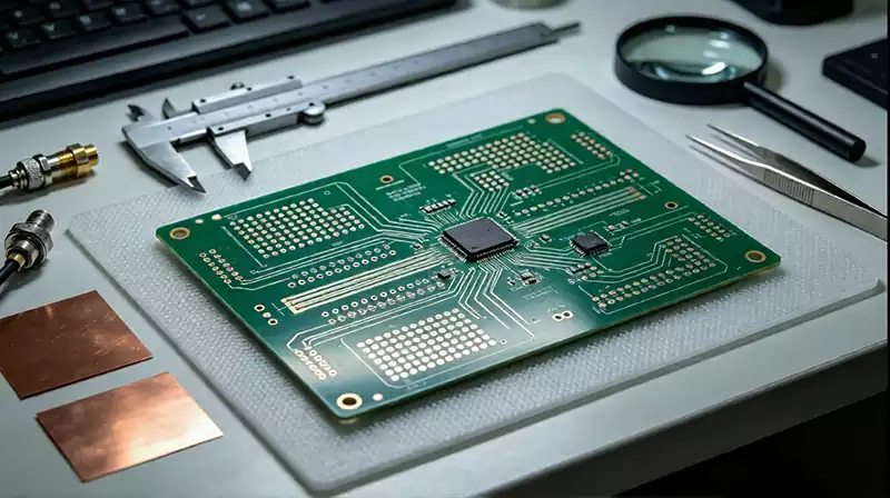
For high-frequency Teflon PCB designs, electrical design and PCB manufacturing must be closely coordinated. The layer stackup should be defined before routing because dielectric thickness and substrate properties directly determine transmission-line impedance.
Impedance control is one of the most critical requirements in RF and microwave circuits. Microstrip and stripline are common controlled-impedance transmission-line structures. Engineers can adjust trace width, copper thickness, and dielectric thickness while accounting for the effective dielectric constant of the laminate to achieve the target characteristic impedance.
As frequency increases, the impact of copper foil surface roughness becomes more significant. Current distribution also changes at high frequencies. Using low-profile or low-roughness copper foil can help reduce conductor loss in certain high-frequency transmission structures.
Via design also requires careful optimization. Oversized or poorly optimized vias can introduce parasitic capacitance and inductance. Via transitions between PCB layers can also create impedance discontinuities and compromise signal integrity. RF layouts commonly use strategically placed ground vias to improve the return-current path and reduce unwanted electromagnetic coupling.
Component placement should follow the RF signal flow. Unnecessary trace bends, excessively long transmission lines, abrupt changes in trace width, and improper reference-plane transitions can all introduce additional discontinuities into the RF signal path.
Applications of Teflon PCBs
Teflon PCBs are used in applications that require low signal loss and stable high-frequency transmission. Radar systems are a typical example. RF signals must propagate reliably through transmission lines and antenna structures, and the PCB substrate can directly affect overall system performance.
Wireless communication equipment is another major application area. RF front-end circuits, filters, antennas, power amplifiers, and various microwave components can benefit from low-loss dielectric substrates.
Teflon PCBs are also used in aerospace and satellite electronics, where stable electrical performance and resistance to demanding operating environments are required. Medical RF equipment, test and measurement instruments, navigation systems, and specialized industrial electronics may also use PTFE-based PCBs when operating frequency and signal integrity requirements are particularly demanding.
Teflon PCB and Impedance Control
Impedance control is one of the most important aspects of high-frequency Teflon PCB design. The characteristic impedance of a transmission line is determined by its trace geometry and surrounding dielectric environment. Therefore, PCB fabrication cannot be separated from the electrical design requirements established during the design stage.
For example, if an engineer specifies a 50-ohm RF transmission line, the PCB manufacturer needs complete stackup information, including dielectric thickness, copper thickness, laminate Dk, trace width, and the overall layer configuration. If the actual dielectric thickness or trace dimensions deviate significantly from the design values, the finished impedance may fall outside the target specification.
For demanding RF applications, impedance should not be treated merely as a parameter shown on the fabrication drawing. It should be managed as a manufacturing control requirement throughout the entire process. Stackup development, material selection, manufacturing tolerances, and impedance testing should be coordinated as part of a single engineering process.
How to Select Teflon PCB Materials
Selecting a Teflon PCB material requires a comprehensive evaluation of operating frequency, target impedance, dielectric thickness, loss requirements, thermal conditions, mechanical constraints, and manufacturing capabilities.
Electrical requirements should be evaluated first. Determine the circuit’s operating frequency and define acceptable insertion loss, impedance tolerance, and signal attenuation limits. Then compare available copper-clad laminates based on their Dk and Df specifications.
The PCB structure is equally important. A simple single-layer RF circuit and a multilayer microwave PCB with multiple controlled-impedance layers have very different requirements. The selected material must be compatible with the proposed stackup, via structure, copper thickness, and manufacturing tolerances.
Cost is also an important consideration. PTFE laminates and their associated manufacturing processes are generally more expensive than standard FR-4 materials. If the circuit does not require low-loss, high-frequency performance, using PTFE unnecessarily can increase manufacturing costs without providing a corresponding electrical benefit.
Teflon PCBs are designed for applications where conventional PCB materials cannot provide the required high-frequency performance. PTFE-based copper-clad laminates offer low dielectric loss and stable electrical characteristics, making them suitable for RF and microwave circuits. They are widely used in radar, wireless communications, aerospace, medical equipment, and other high-frequency electronic applications.