Winning at the Starting Line: How to Cut Hidden Costs Through Design for Manufacturability (DFM)
In the business world of electronics manufacturing, many clients often focus the majority of their energy on schematic design and software debugging during product development. Only when the circuit board design is complete and ready for production do they hand the drawings to the PCB manufacturer and foundry (EMS), saying, “Give me a quote; I need the cheapest solution.” But how to make a Cost Efficient PCB Assembly?
However, 80% of the product’s manufacturing cost is locked in the moment the engineer draws the last PCB trace and finalizes the BOM (Bill of Materials). If cost-efficient PCB assembly thinking isn’t incorporated from the initial design stage, subsequent price reductions through negotiations with foundries and chip distributors will be minimal. In fact, basic design errors in the early stages can lead to frequent production line shutdowns, board rework, and large-scale scrap.
True masters utilize precise Design for Manufacturability (DFM) to minimize the manufacturing complexity for contract manufacturers during the design phase, thereby eliminating unnecessary hidden costs at the source.
The Art of Panelization: Squeezing Every Inch of Board Material into Its Residual Value
In the raw material cost of printed circuit boards, the cost of the board material (such as FR4 substrate) is calculated based on the area of the entire large board. If your individual boards are very small or oddly shaped (such as round, L-shaped, or irregularly shaped boards with various uneven edges), sending them directly to the assembly line as single pieces will not only be difficult for the pick-and-place machine’s robotic arm to handle, but they are also highly prone to tipping over during high-temperature reflow soldering.
This is where “panelization design” comes in. Panelization is not simply putting several boards together; it involves extremely sophisticated operational research.
With proper panelization planning, we can perfectly lay individual PCBs on standard bulk materials from the PCB manufacturer, reducing waste from scrap to below 5%. Simultaneously, we add a universal “routing border” around the panelization and mark this border with Automated Optical Inspection (AOI) and fiducial marks for pick-and-place machines.
This transforms single PCBs, which previously required frequent loading and unloading, into large boards that can be assembled in batches, instantly increasing production line throughput several times over. For foundries, processing fees are based on “operational time” and “number of loading and unloading operations.” With a dozen boards assembled in a single load, the processing cost per PCB drops dramatically, achieving basic cost-efficient PCB assembly.
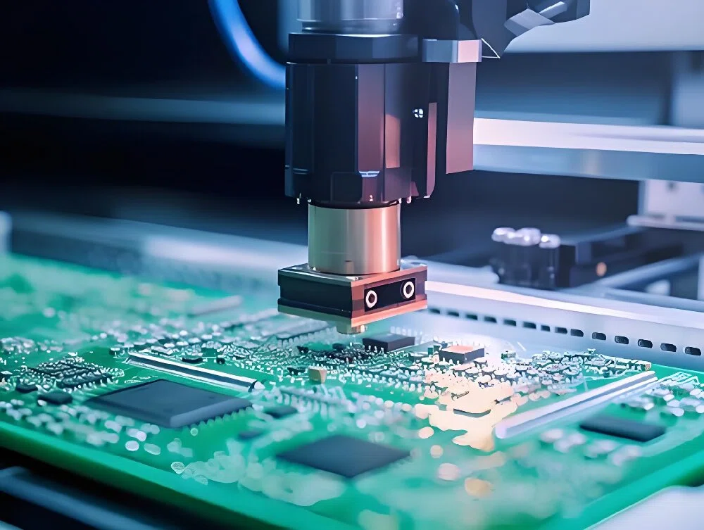
The “uniform” component layout eliminates unnecessary secondary reflow soldering. When working, a pick-and-place machine is like a high-speed machine gun. Its nozzle picks up components from the tape, then spins rapidly and places them onto the pads of the circuit board. If your PCB design has components haphazardly positioned—some horizontal, some vertical, some at a 45-degree angle—the pick-and-place machine head must frequently brake, rotate, and realign during its movement. This not only significantly slows down the placement speed and extends production time but also increases the probability of component rejection (components falling off due to unstable pickup) due to high-frequency mechanical vibration.
Worse still, if engineers, in pursuit of so-called “compactness,” densely pack surface-mount components (SMDs) across both sides of the circuit board without any pattern, the foundry must resort to two expensive high-temperature reflow soldering processes: first, placing the front side and reflowing it in the oven; then flipping it over to place the back side and reflowing it again. Furthermore, if the back side also contains a large number of through-hole (THT) components, manual soldering or expensive selective wave soldering must be used.
To achieve optimal cost-effectiveness, the best layout strategy should be to concentrate all high-density core components (such as CPUs, BGAs, and large capacitors) on the same side of the circuit board (the main side).
If components must be placed on the back side, only place extremely small passive components such as resistors and capacitors that are not prone to falling off at high temperatures. Simultaneously, ensure that all components of the same type (such as all 0603 resistors) have perfectly parallel long axes. This allows the pick-and-place machine to complete single-sided placement at top speed, simplifying the expensive and complex double-sided soldering process to standard single-sided soldering, resulting in a significant leap in production line efficiency.
The Cost Game of BGA Soldering and Via Design (Avoiding High-Risk Process Pitfalls)
In Chapter 1, we mentioned using DFM to optimize overall layout and panelization. In this chapter, we must delve into the more microscopic process level, discussing the two “bottomless pitfalls” that hardware engineers are most prone to fall into and that cause the most headaches for foundry owners: via design in the BGA area and thermal isolation of component pads. The quality of handling these two points directly determines the first-pass yield (first-time pass rate) of soldering.
Via-in-Pad or Dog Bone? A Life-or-Death Choice Between Cost and Yield
As discussed in our previous technical teardown, when chip pins are too dense, engineers often use “via-in-pad” technology, directly placing vias onto the BGA pads.
However, during engineering evaluations, it’s crucial to emphasize that vias are “poison” for high-efficiency surface mount technology. Unless space is truly unavoidable, they should be avoided at all costs in projects prioritizing cost-effectiveness.
This is because using vias requires PCB manufacturers to add three arduous additional processes to prevent molten solder paste from leaking into the vias during reflow soldering and causing cold solder joints: resin plugging, surface grinding, and secondary copper plating (POFV). This not only causes the purchase price of the bare PCB carrier to surge by 30% to 50%, but also extends lead times due to the longer process chain. To achieve cost-efficient PCB assembly, the best alternative is to use “blind vias” or standard “dog-bone fanouts” around the chip. These vias are led out of the pads via a short trace and then covered with solder mask (green solder mask). This saves PCB manufacturers the expensive cost of resin plugging and prevents solder paste leakage, allowing even the most basic surface mount production lines to achieve an ultra-high soldering yield of 99.9%.
The “Tombstoning” Disaster on Large Copper Areas and Thermal Isolation Pads
In PCB design, large areas of ground (GND) or power (PWR) copper are often laid to enhance conductivity and heat dissipation. If one end of a small resistor or capacitor is connected to a thin, ordinary trace, while the other end is directly connected to a large copper area, disaster is brewing.
When the PCB enters the reflow oven, the entire board begins to heat up. The solder pads connected to the thin traces heat up extremely quickly because there’s no excess metal around them to absorb heat. The solder paste there melts in just 10 seconds, creating an inward surface tension. However, the solder pads connected to the large copper area act like giant heat sinks, rapidly absorbing heat, causing the temperature to rise very slowly. The solder paste doesn’t begin to melt until 20 seconds later.
This 10-second time difference creates a bizarre physical phenomenon: the pulling force from the first melting end violently “pulls” one end of the lightweight resistor or capacitor upwards, making it stand upright on the circuit board like a tombstone. This is the industry-famous “tombstoning effect.”
Once tombstoning occurs, the entire board will experience a broken circuit during functional testing. The foundry must deploy a large number of manual repair workers, using soldering irons under microscopes, to manually straighten and resolder each component. This manual rework is extremely costly, directly destroying the efficiency of automated production.
To eliminate this hidden cost, the method is very simple and requires no additional expense: enforce a “cross-shaped thermal relief” design on all component pads connecting large copper areas.
Four thin copper bridges isolate the pads from the surrounding large copper areas. These four small bridges are both conductive and effectively prevent rapid heat loss, allowing the pads at both ends of the component to melt at the same temperature when entering the furnace. Without temperature differences, the components sit securely, enabling automated production lines to operate efficiently with zero rework.
The Art of Simplifying the Supply Chain and Bill of Materials (BOM)
Having optimized layout and micro-processes by eliminating premiums through standardization, the next crucial element determining the project’s success or failure is the densely packed Bill of Materials (BOM). In the electronic component procurement chain, quantity is justice, and standardization is freedom.
Rationalization: Eliminating Loose Components and High Downtime Costs for Replacement. Many hardware engineers lacking practical production experience are very casual when designing circuits. For example, when drawing circuits, they might use a 5.1K ohm resistor here and a 4.7K ohm resistor there; or for decoupling capacitors, they might use 0.1uF one moment and 0.22uF the next. While theoretically these tiny differences in resistance or capacitance can bring certain local performance of the circuit to a so-called “perfect limit,” in actual production, this lack of a normalized BOM is a procurement and production disaster. The number of feeders that a foundry’s placement machine can hold is limited.
If your BOM includes 50 different sizes of tiny resistors and capacitors, the foundry must fill 50 reels of parts on the machine. Procurement Disadvantages: 50 different materials mean procurement staff have to place 50 orders with different suppliers, buying only a few hundred units of each material, making it impossible to obtain bulk purchase discounts, and even incurring minimum order quantity (MOQ) fees for each loose component. Production Disadvantages: Once a material is used up, the production line must stop, requiring workers to climb onto the machine to replace the reel. Every minute the pick-and-place machine is down means significant idle labor costs for the customer.
The true way to achieve cost-efficient PCB assembly is to enforce material standardization. During design reviews, all resistance and capacitance values that do not affect core performance are uniformly merged. If 4.7k can be used instead of 5.1k; if 0.1uF can be used consistently, nothing more is added. Ultimately, a BOM containing hundreds of messy passive components is streamlined and compressed to only a dozen or so common models. This resulted in a dramatic increase in procurement quantities, from a few hundred units of each type to tens of thousands, allowing them to obtain bulk wholesale prices from the original manufacturers. Simultaneously, the pick-and-place machine only needed a few general-purpose feeders to operate at full speed, eliminating the need for any downtime for material changes, thus drastically reducing production labor costs.
Embracing General-Purpose Packaging: Saying Goodbye to the “Premium Black Hole” of Niche Components When selecting active components (such as microcontrollers, operational amplifiers, and interface chips), the choice of packaging is equally crucial. Some new chips, in pursuit of so-called “ultra-thin” designs, employ extremely aggressive BGA or leadless QFN/DFN packages. These packages not only result in high chip prices but also impose incredibly stringent requirements on soldering and testing. For example, the pins of a QFN package are all hidden on the underside of the chip; after reflow soldering, ordinary AOI (Automated Optical Inspection) equipment cannot clearly see whether the solder joints on the bottom are faulty.
To ensure quality, foundries must mandate expensive X-ray inspection at the back end of the production line. Using an additional high-end inspection device will increase the processing cost per board by a few dollars. When space permits, try to persuade customers to choose SOP, TSSOP, or large-pitch QFP packages, which are technologically mature, have readily available alternatives, and have exposed pins. These established general-purpose packages are not only extremely inexpensive in terms of materials, but also allow foundries to perform 100% visual inspection of solder joints in milliseconds using even the most basic camera-based AOI, completely eliminating the need for expensive X-rays. This approach of “using general-purpose processes to outperform niche, high-precision technologies” is the highest wisdom in supply chain management.
Matching Foundries (EMS) and Production Line Alignment Strategies
After completing all the design and material preparation, the final cost-saving trick lies in how you select and manage your foundry. Larger or more advanced foundries are not necessarily better; the key is “matching the right company.”
Avoid the “tail-end project” trap of large manufacturers and find a matching gold-standard processor. Many startups and small-to-medium-sized clients have a misconception: they believe that entrusting projects to top global industry giants (such as Foxconn, Jabil, and JCET) is the safest bet.
However, reality is harsh. If your order volume is only a few hundred or a few thousand units, in the eyes of those large manufacturers with dozens of world-class ultra-high-speed production lines, you are merely a “micro-tail project,” barely enough to fill a gap in their supply chain.
Price discrimination: Because your order volume cannot fill their capacity, they will charge you extremely high “native prototype setup fees (NRE)” and production scheduling premiums.
Indifferent service: Large manufacturers’ top engineering teams and high-precision equipment will prioritize serving giants like Apple and Nvidia. Your project will most likely be assigned to the most peripheral, oldest, and least experienced backup slow production lines, where waiting for support for technical issues could take weeks.
Therefore, the core of pursuing cost-efficient PCB assembly is to choose mid-sized specialized contract manufacturers with excellent equipment, standardized management, and who treat your order size as a “VIP core customer.” In a mid-sized factory, your order of several thousand units is their factory’s key project for the entire month. Their best process engineers (PEs) and production supervisors will monitor your production line throughout the process, adjusting processes based on feedback. Not only are their prices only half or even a third of those of large manufacturers, but their communication efficiency and response speed are also significantly superior.
The Business Psychology of Production Line Tuning: Streamlining Mass Production and Testing Solutions. Every action a contract manufacturer takes on the production line represents real labor costs. In the final assembly and testing stages, we must strive to avoid “manual dependence.”
If, after your product is surface-mounted, you still need to manually touch each test point with a test probe, or manually plug and unplug various connectors while waiting for several minutes for the programming process, this process is not only extremely inefficient but also prone to missed tests due to worker fatigue.
An efficient approach is for hardware engineers to pre-define a row of neat “test points” on the PCB and provide the foundry with a “bed of needles test fixture (FCT Fixture)” that can be run automatically with a single click.
As soon as the board is placed on the plate, the clamp presses down, and dozens of spring probes instantly contact all test points. The computer automatically completes the programming, voltage and current detection, and functional determination within one second, and automatically prints out a pass label. Through this complete automation and “foolproofing” of manual testing, contract manufacturers no longer need highly paid skilled technicians sitting at the end of the production line wasting time. A single, ordinary frontline operator can complete the rapid testing. By saving contract manufacturers labor time, you naturally gain the absolute leverage to negotiate extremely low assembly quotes.