With the rapid evolution of 5G/6G communications, optoelectronic displays, high-end microelectronics and aerospace technology, traditional PCB substrates are no longer able to meet the stringent requirements of high-end equipment, such as high-temperature resistance, high-frequency stability, optical transparency and high dimensional accuracy. Thanks to their unique physical, chemical and optical properties, glass substrates have become the core substrate material for new high-end PCBs.
Selection of glass substrates
Fused Quartz Glass
Capable of withstanding extreme temperatures of up to 1,000°C, it has an extremely low coefficient of thermal expansion (approximately one-tenth that of ordinary glass) whilst maintaining excellent optical transparency across the ultraviolet to near-infrared spectrum. It is suitable for use as a core substrate in laser instruments, high-temperature sensors and semiconductor equipment, and is able to maintain precise alignment of circuit patterns even under drastic temperature fluctuations.
Microcrystalline Glass
Produced through a controlled crystallisation process, it combines the processability of glass with the dimensional stability of ceramics. It has a low dielectric constant (typically 4–5, significantly lower than FR4’s 4.5–5.5 and with minimal frequency-dependent variation) and a low dielectric loss tangent, effectively reducing transmission attenuation and phase shift in high-frequency signals. It is an ideal choice for 5G base station antennas, millimetre-wave radar and satellite communication systems.
Sapphire Glass
With a hardness second only to diamond, it offers excellent chemical resistance and transparency in the infrared spectrum. Although costly, sapphire glass PCBs are virtually irreplaceable in military infrared detection windows, high-power lasers and optical imaging equipment operating in extreme environments.
Tempered Glass
Treated via chemical or thermal tempering processes, its mechanical strength is significantly enhanced, offering excellent impact and vibration resistance. It is suitable for applications with stringent reliability requirements, such as rugged outdoor surveillance equipment, night vision devices and vehicle electronic control units, ensuring that internal circuits remain intact even when subjected to drops or severe vibrations.
Epoxy Glass (FR4 Glass PCB)
Using glass fibre cloth impregnated with epoxy resin as the substrate, this offers outstanding value for money and moderate heat resistance (long-term operating temperature of approximately 130–150°C). It retains the ease of processing and low cost of traditional FR4, whilst offering lower moisture absorption and better dimensional stability than standard FR4. It is the most widely used ‘affordable’ glass PCB in fields such as consumer electronics and general industrial control.
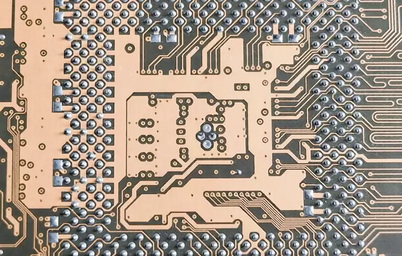
Glass Substrate Manufacturing Process
1.Material Preparation and Surface Treatment
Thorough cleaning of the glass substrate is key to ensuring the adhesion of subsequent coatings. Manufacturers first use an ultrasonic cleaning process to remove micron-sized dust and debris, followed by chemical cleaning using alkaline cleaning solutions, deionised water and solvents such as isopropyl alcohol. Finally, the substrate is dried in a clean environment to ensure the surface is free of any oil or oxides.
2.Photolithography Process
A photoresist material (a polymer sensitive to ultraviolet light, available in positive and negative types) is spin-coated or spray-coated onto the surface of the cleaned glass substrate. Subsequently, a mask bearing the circuit design pattern is placed over the substrate and selectively exposed to ultraviolet light. After exposure, a developer is used to dissolve the uncured areas of the photoresist, leaving precise ‘windows’ of the circuit pattern on the glass surface. The minimum line width achievable with this process can be controlled to within 10 micrometres, meeting the requirements for high-density interconnections.
3.Application of the Conductive Layer
This is one of the core challenges in glass PCB manufacturing. As the glass surface is smooth and non-conductive, it cannot be electroplated directly. Manufacturers typically employ physical vapour deposition (such as sputtering or thermal evaporation) or electroless plating methods. First, an extremely thin seed layer (such as titanium + copper) is deposited, followed by electroplating to build up the copper to the required thickness (typically 1–35 micrometres). This process requires strict control of temperature and stress to prevent the glass substrate from fracturing due to thermal mismatch.
4.Drilling and Via Formation
When the design requires multi-layer electrical interconnections, holes must be drilled in the glass substrate. Traditional mechanical drilling is prone to causing chipping or cracking of the glass; therefore, the industry generally employs CO₂ laser or UV laser drilling technologies. The laser beam can be precisely focused to a diameter of tens of micrometres, instantly vaporising the glass material to form smooth hole walls. Conductive metal is then deposited on the inner walls of the holes via electroless plating or sputtering processes, creating reliable electrical vias.
5.Finishing and Coating Processes
Finally, a protective layer is applied to the surface of the glass PCB after the circuit has been fabricated. Common surface treatments include: electroless nickel-gold (ENIG, used to enhance soldering reliability and solderability), solder mask (used to prevent solder bridging and oxidation), and conformal coatings (such as acrylic or poly(p-xylene), used for moisture and dust protection). For transparent glass PCBs, transparent or light-coloured inks are typically used for the solder mask to preserve their optical properties.
Key Advantages of Glass Substrates
1.Excellent high-temperature resistance
Traditional FR4 circuit boards typically have a glass transition temperature of only 130–180°C; once this temperature is exceeded, the substrate softens, expands and may even decompose rapidly. In contrast, fused silica glass PCBs can withstand temperatures of up to 1,000°C and exhibit virtually no deformation during thermal cycling. This makes them an ideal choice for high-temperature applications such as 3D printer heating heads, electronic modules in automotive engine compartments and heat dissipation substrates for power LEDs.
2.Stable High-Frequency Signal Transmission
The dielectric constant (Dk) of glass is typically 4–6, with minimal variation with frequency; the dielectric loss factor (Df) can be as low as 0.002–0.005, far lower than the approximately 0.02 of FR4. This means that in 5G millimetre-wave (24–100 GHz), RF front-end and radar systems, glass PCBs can effectively reduce signal attenuation, delay and crosstalk, significantly improving communication quality and system sensitivity.
3.Optical Transparency
This is the core feature that distinguishes glass PCBs from all traditional circuit boards. By selecting transparent glass substrates and transparent or patterned conductive materials (such as indium tin oxide (ITO) or ultra-thin metal grids), it is possible to achieve truly transparent circuits. These ‘invisible’ circuits ensure electrical functionality whilst not obstructing the display content or ambient light behind the device, and are widely used in transparent smartphones, transparent LED displays, smart windows, and automotive head-up displays. Some transparent glass PCBs can also be combined with edge-lit LEDs to achieve 360° uniform illumination, offering entirely new possibilities for creative lighting fixtures and decorative lighting.
4.Exceptional chemical and dimensional stability
Glass inherently resists chemical agents such as acids, alkalis and organic solvents, and has virtually zero water absorption (compared to FR4, which absorbs approximately 0.1–0.5%). Furthermore, the thermal expansion coefficient of glass (approximately 3–5 ppm/°C) is very close to that of silicon chips (approximately 2.6 ppm/°C) and significantly lower than that of FR4 (approximately 14–17 ppm/°C). This means that glass PCBs will not warp, buckle or suffer delamination between layers in response to temperature changes or in humid environments, enabling them to operate reliably over the long term under harsh conditions such as the high magnetic fields inside MRI scanners or the high-pressure saline environments of deep-sea exploration equipment.
5.Slim and Lightweight Design
As electronic products such as smartphones, smartwatches and medical implantable devices become increasingly compact and lightweight, the minimum thickness of traditional FR4 boards is typically limited (thicknesses below approximately 0.2–0.4 mm are fragile and difficult to process). In contrast, thin glass substrates (such as chemically strengthened glass) can be manufactured to thicknesses as low as 0.1 mm or even 0.05 mm, whilst maintaining sufficient rigidity and flatness. This characteristic not only saves valuable stacking space within devices but also provides a circuit substrate for innovative form factors such as foldable smartphones and ultra-thin wearable devices.
Applications of Glass Substrates
Aerospace
Satellite communication modules, radar signal receivers and flight control computers must withstand severe vibrations during launch, extreme temperature fluctuations in space (–200°C to +150°C) and high-energy particle radiation. Thanks to their excellent radiation resistance, low outgassing rates and dimensional stability, glass PCBs have become a reliable choice for the next generation of aerospace electronic systems.
Optoelectronics
In optical sensors, optical communication transceiver modules and LED lighting equipment, the light-transmitting properties of glass-based PCBs can significantly improve light coupling efficiency. For example, by directly flip-mounting optoelectronic chips onto transparent glass PCBs, light can pass through the substrate into the chip or out from the chip, reducing losses in intermediate media and optimising the device’s signal-to-noise ratio and optical output power.
Microelectronic Packaging
Glass PCBs possess extremely high surface flatness (sub-micron level) and a coefficient of thermal expansion close to that of silicon, making them an ideal substrate for high-density microelectronic packaging. In chip-scale packaging (CSP), three-dimensional integrated circuits (3D ICs) and fan-out wafer-level packaging, glass interlayers enable finer line widths/spacing (≤2 micrometres) and lower interconnect delay, helping to further reduce system size and increase bandwidth.
RF and Microwave Equipment
The low dielectric loss and stable dielectric constant of glass PCBs make them particularly suitable for the design of RF front-end modules, millimetre-wave antenna arrays, and automotive collision-avoidance radar. In these applications, every 0.5 dB reduction in signal transmission loss translates to a significant improvement in communication range or detection sensitivity. Consequently, glass PCBs are gradually replacing traditional high-frequency substrates (such as PTFE composites) and have been field-tested in 5G base stations, satellite ground terminals and military radar systems.
Glass substrates are not simply a combination of ‘glass and circuits’, but rather a technological system encompassing a variety of specialised glass materials, precision photolithography and coating, and laser micro-drilling. Although the cost of glass PCBs currently remains higher than that of traditional PCBs, and the yield rate for large-size processing needs to be improved, the industrialisation of glass PCBs is bound to accelerate with the rapid development of 5G/6G communications, autonomous driving, wearable medical devices and transparent display technologies.